Digital i/o pins, Los, losout, In1, rsel, out1, rselout – Rainbow Electronics DS1874 User Manual
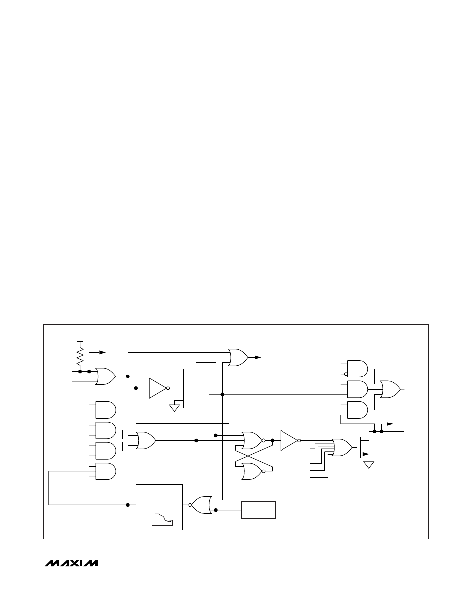
Page 21: Txf, txd, txdout, Figure 12. logic diagram 1, Ds1874 sfp+ controller with digital ldd interface
DS1874
SFP+ Controller with Digital LDD Interface
______________________________________________________________________________________
21
Digital I/O Pins
Five digital input and five digital output pins are provid-
ed for monitoring and control.
LOS, LOSOUT
By default (LOSC = 1, Table 02h, Register 89h), the
LOS pin is used to convert a standard comparator out-
put for loss of signal (LOS) to an open-collector output.
This means the mux shown in the
Block Diagram
by
default selects the LOS pin as the source for the
LOSOUT output transistor. The output of the mux can
be read in the STATUS byte (Table 01h, Register 6Eh)
as the RXL bit. The RXL signal can be inverted (INV
LOS = 1) before driving the open-drain output transistor
using the XOR gate provided. Setting LOSC = 0 config-
ures the mux to be controlled by LOS LO, which is dri-
ven by the output of the LOS quick trip (Table 02h,
Registers BEh and BFh). The mux setting (stored in
EEPROM) does not take effect until V
CC
> POA, allow-
ing the EEPROM to recall.
IN1, RSEL, OUT1, RSELOUT
The digital input IN1 and RSEL pins primarily serve to
meet the rate-select requirements of SFP and SFP+.
They also serve as general-purpose inputs. OUT1 and
RSELOUT are driven by a combination of the IN1,
RSEL, and logic dictated by control registers in the
EEPROM (Figure 13). The levels of IN1 and RSEL can
be read using the STATUS register (Lower Memory,
Register 6Eh). The open-drain output OUT1 can be
controlled and/or inverted using the CNFGB register
(Table 02h, Register 8Ah). The open-drain RSELOUT
output is software-controlled and/or inverted through
the Status register and CNFGA register (Table 02h,
Register 89h). External pullup resistors must be provid-
ed on OUT1 and RSELOUT to realize high logic levels.
TXF, TXD, TXDOUT
TXDOUT is generated from a combination of TXF, TXD,
and the internal signal FETG. A software control identi-
cal to TXD is available (TXDC, Lower Memory, Register
6Eh). A TXD pulse is internally extended (TXD
EXT
) by
time t
INITR1
to inhibit the latching of low alarms and
warnings related to the APC loop to allow for the loop to
stabilize. The nonlatching alarms and warnings are TXP
LO, LOS LO, and MON1–MON4 LO alarms and warn-
ings. In addition, TXP LO is disabled from creating
FETG. TXF is both an input and an output (Figure 12).
See the
Transmit Fault (TXF) Output
section for a
detailed explanation of TXF. Figure 12 shows that the
C
C
D
Q
Q
S
R
OUT
IN
TXDS
R
PU
TXF
SET BIAS REGISTER TO 0 AND
MAX3798/MAX3799
SET_IMOD TO 0
TXD
MINT
HBAL FLAG
TXP LO FLAG
TXP LO FLAG
BIAS MAX FLAG
TXP HI FLAG
TXP HI ENABLE
BIAS MAX
BIAS MAX ENABLE
HBAL FLAG
HBAL ENABLE
TXP LO FLAG
TXP LO ENABLE
TXD
EXT
TXDC
V
CC
TXD
TXF
TXDOUT
TXDIO
TXDFG
FETG
TXDFLT
FAULT RESET TIMER
(130ms)
IN
OUT
POWER-ON
RESET
Figure 12. Logic Diagram 1