Ds1874 sfp+ controller with digital ldd interface – Rainbow Electronics DS1874 User Manual
Page 51
DS1874
SFP+ Controller with Digital LDD Interface
______________________________________________________________________________________
51
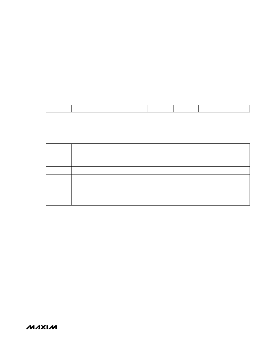
Table 01h, Register FAh: ALARM EN
1
POWER-ON
VALUE
00h
READ ACCESS
PW2 or (PW1 and RWTBL1C) or (PW1 and RTBL1C)
WRITE ACCESS
PW2 or (PW1 and RWTBL1C)
MEMORY TYPE
Nonvolatile (SEE)
FAh RESERVED RESERVED RESERVED RESERVED
HBAL
RESERVED
TXP
HI
TXP
LO
BIT
7
BIT
0
Layout is identical to ALARM
1
in Lower Memory, Register 72h. Enables alarms to create internal signal FETG (see
Figure 12) logic. The MASK bit (Table 02h, Register 89h) determines whether this memory exists in Table 01h or
05h.
BITS
7:4
RESERVED
BIT
3
HBAL:
0 = Disables interrupt from HBAL alarm.
1 = Enables interrupt from HBAL alarm.
BIT
2
RESERVED
BIT
1
TXP HI:
0 = Disables interrupt from TXP HI alarm.
1 = Enables interrupt from TXP HI alarm.
BIT
0
TXP LO:
0 = Disables interrupt from TXP LO alarm.
1 = Enables interrupt from TXP LO alarm.