Experiment #42: “nor” gate using ttl, Experiment #84: logic testing circuit – Elenco 130-in-1 Electronics Playground User Manual
Page 58
-58-
Try to mark 0 and 1 inputs on the schematic and see
if this circuit comes up at either a 0 or 1 output. Give
it try and don’t peak at the answer.
As you are constructing this circuit, make sure to
have the switch set to B. Once you have completed
the wiring, connect to terminals 13 and 14. Now
press the key. Are there any changes in LED 1? Now
release the key and place the switch to A. Now what
occurs on LED 1? Leave the switch at A and then
press the key. Is anything different occurring?
This project acts just like the other NOR gates we
have built. The NANDs mark with an A and B both
have an input of 1. Therefore they both have an
output of 0 when the input is 1. Their outputs are
used as inputs to the NAND labeled C. The output of
NAND C is 1 as long as one or both of inputs are 0.
This output is used for the inputs of the next NAND
causing it to have an output of 0. Therefore the LED
1 does not light.
A NOR gate only has an output of 1 when both inputs
are 0. This occurs when the switch is set to B and the
key is not pressed.
Notes:
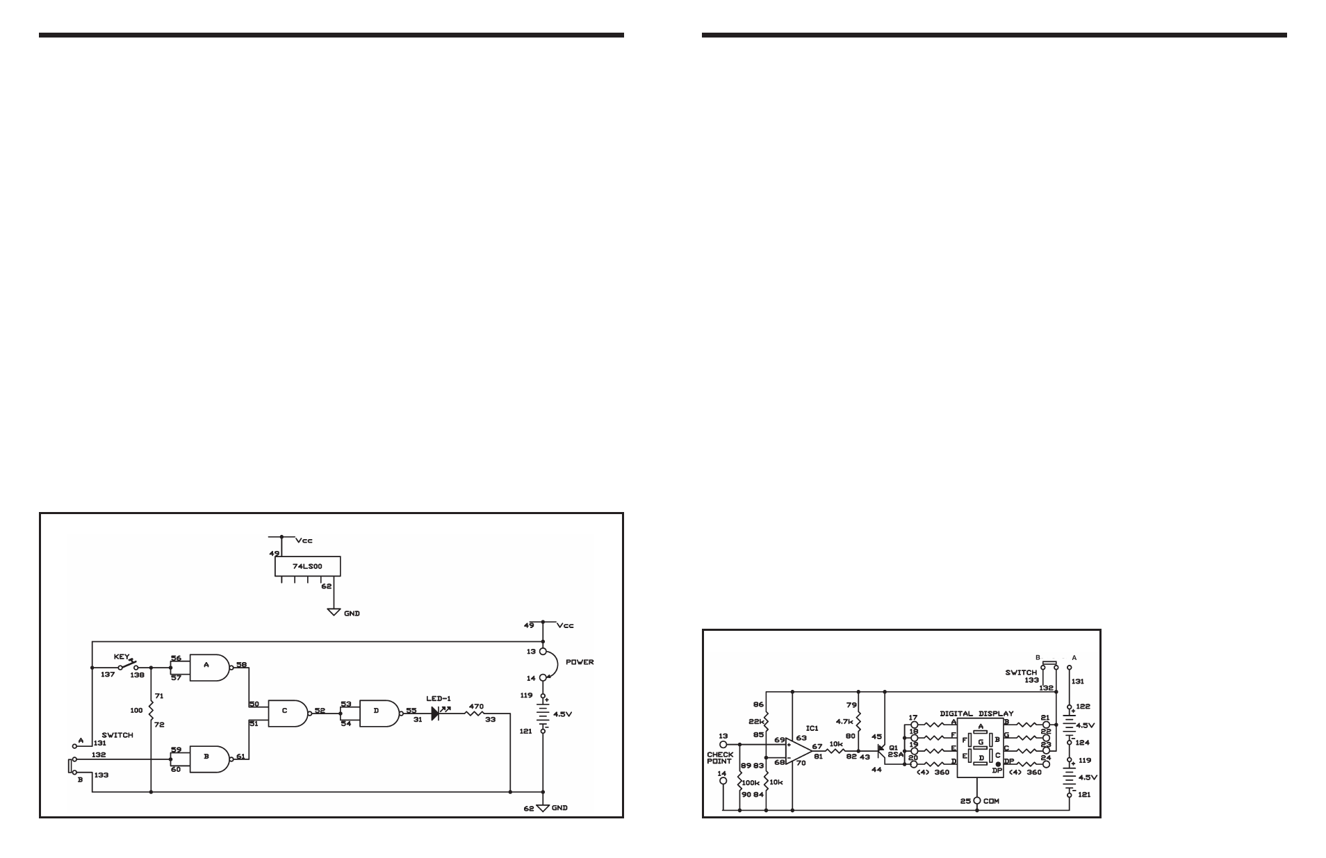
EXPERIMENT #42: “NOR” GATE USING TTL
Wiring Sequence:
o 13-49-131-137
o 14-119
o 31-55
o 72-33-62-133-121
o 50-58
o 51-61
o 52-53-54
o 56-57-71-138
o 59-60-132
o 13-14 (POWER)
Schematic
-103-
You know that digital circuits produce low or high (L
or H) outputs (0 or 1). Now you’re going to create a
logic tester that shows 1 for high level (H) and 0 for
low level (L) on the LED display.
Slide the switch to position B and construct the
circuit. When you finish the wiring, slide the switch to
position A to turn on the power. The number 0 is on
the display because the test terminal (terminal 13) is
at low level when no input is exerted. Attach the test
terminal-to-terminal 122 to apply +4.5V. The display
alters to 1.
View the schematic. The operational amplifier works
as a comparator. The 22k
Ω and 10kΩ resistors
produce a reference voltage of 3V at its negative (-)
input terminal. When the voltage at its positive (+)
terminal exceeds this reference voltage, the
comparator’s output level goes high, turning off
transistor Q1. Now segments A, D, E, and F on the
display turn off, leaving a 1 on the display.
Notes:
EXPERIMENT #84: LOGIC TESTING CIRCUIT
Wiring Sequence:
o 17-18-19-20-44
o 86-79-63-21-23-45-132
o 43-80-82
o 67-81
o 68-83-85
o 119-124
o 122-131
o 69-89-13-CHECK POINT
o 121-25-70-90-84-14-CHECK POINT
Schematic