Experiment #39: “triple-input and” gate using ttl, Experiment #87: sweep oscillator – Elenco 130-in-1 Electronics Playground User Manual
Page 55
-55-
We have been using digital circuits that have two
inputs, but that doesn’t mean that we can’t have
more than the two inputs. Here is a TTL AND gate
which has three inputs. Use the schematic to try and
figure out how to have three inputs result in an output
of 1.
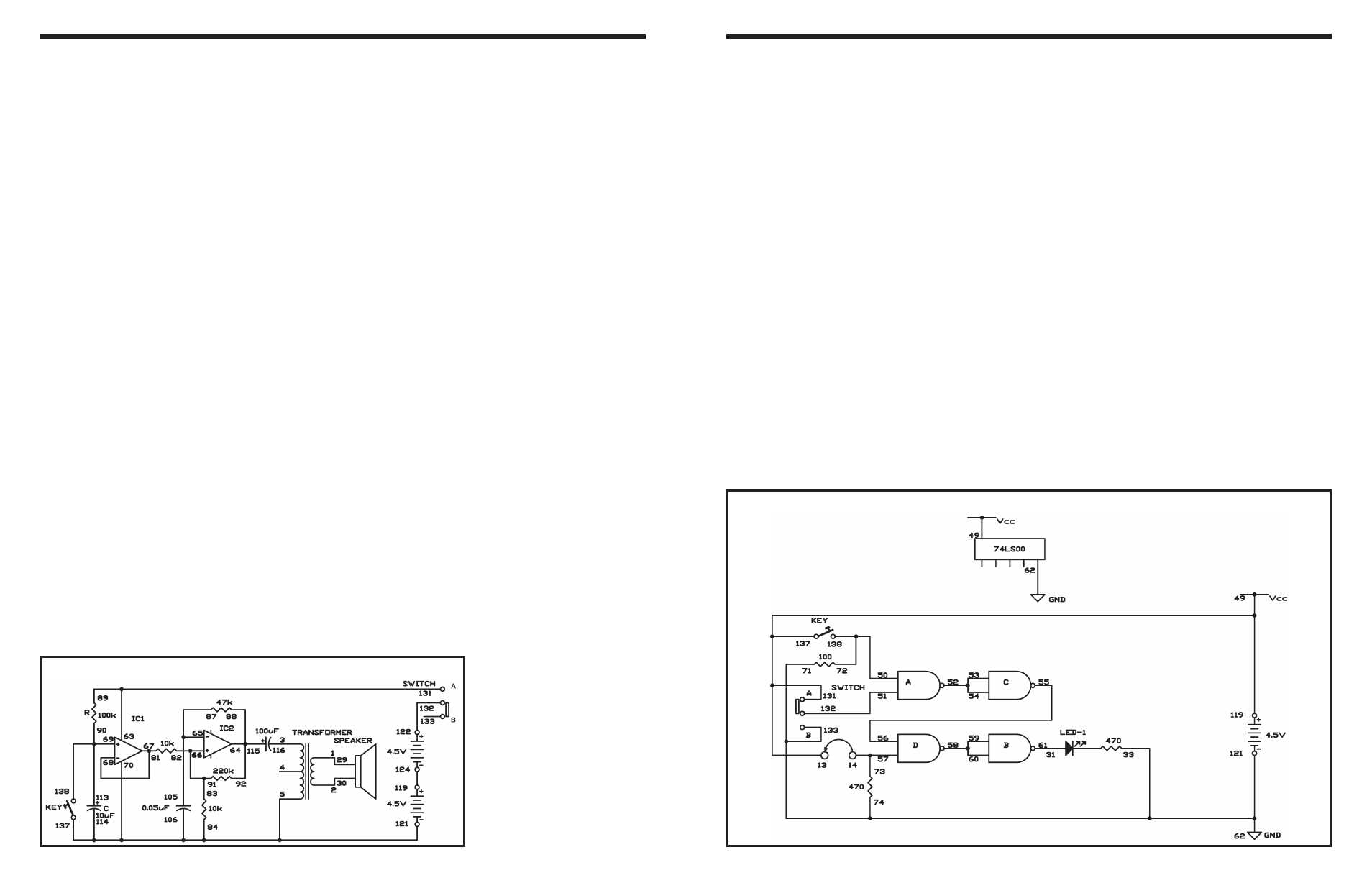
We are going to do things a bit differently this time -
terminals 13 and 14 create P as an input signal.
When you connect the two terminals they create a 1
input, and disconnecting them creates a 0.
Connecting terminals 119 and 137 “turns on” this
project.
This circuit is called a gate because it is a circuit that
has more than one input and only one output. The
output of the gate is not energized until the inputs
meet the certain requirements. We will be using this
handy component in more digital circuits through
other projects.
A gate circuit that is used to keep two portions of a
circuit separated from each other is called a buffer.
Next, look at the schematic and see if you can figure
out the connections needed for the switch, the key,
and terminals 13 and 14 that will result in an output
of 1. Try to figure it out on your own and then read on
to see if you were correct.
The circuit works this way: connected to the one
NAND are both the key and the switch. When each
provides an input of 1, then the NAND has an output
of 0. This 0 creates the input of another NAND,
causing the output to become 1.
This output of 1 then goes on to another NAND gate
(can you find it on the schematic?). There it makes
up one input in addition to the input from terminals
13 and 14 that created the other. Once these inputs
are both 1, then the NAND’s output goes to 0. This
output is used with both of the inputs of the last
NAND, thus causing it to become 1 and for the LED
to light.
Doesn’t it seem simple? Well, believe it or not but,
even complex computers operate through the use of
the same principles we are using in these circuits.
Notes:
EXPERIMENT #39: “TRIPLE-INPUT AND” GATE USING TTL
Wiring Sequence:
o 13-49-131-137-119
o 14-73-57
o 31-61
o 74-71-62-33-121-133
o 50-72-138
o 51-132
o 52-53-54
o 55-56
o 58-59-60
Schematic
-106-
The electronic buzzer we built in the previous circuit
can only make a continuous beep, but we can make
a similar circuit that produces various siren sounds.
Your going to make a siren that gives out a sound
with a variable pitch. When you move the switch, this
siren wails and then creates a continuous high-
pitched noise.
Slide the switch to position B and assemble the
circuit. When you complete the wiring, turn the power
on by sliding the switch to position A. You hear the
speaker produce a sudden, roaring siren sound. At
first the sound is low and becomes higher, then
changes to a steady tone in about 3 to 4 seconds.
When you press the key and release it, the capacitor
discharges and starts the siren sound again.
You can understand how this works by looking at the
schematic. The pitch changes as the 10
μF capacitor
is charged through the 100k
Ω resistor. IC 2 is an
astable multivibrator. IC 1 is a buffer between the
capacitor and IC 2.
Notes:
EXPERIMENT #87: SWEEP OSCILLATOR
Wiring Sequence:
o 1-29
o 2-30
o 3-116
o 5-84-70-106-114-137-121
o 89-63-131
o 64-88-92-115
o 65-87-105
o 66-82-83-91
o 68-67-81
o 90-69-113-138
o 119-124
o 122-132
Schematic