Experiment #97: voice power meter – Elenco 130-in-1 Electronics Playground User Manual
Page 44
-117-
-44-
In this circuit you will first learn about the AND circuit.
When all the connections to its terminals are logic
high (receiving voltage), the AND circuit produces a
high output.
Make the connections in this circuit based upon the
wiring sequence below. After that make the
connection to terminals 119 and 124 using terminals
A (126) and B (128) in different combinations to
complete the circuit and to learn how an AND circuit
works.
Terminal 124 provides logic high (voltage) while
terminal 119 provides logic low (no voltage) in this
circuit. H is only shown on the LED after you have
connected terminal A and terminal B to terminal 124
(high terminal). If you make the connection of either
terminal A or B or both to terminal 119 (low terminal)
the LED will display nothing. For the combined output
(the LED) to read H (high), both A and B have to be
high.
The PNP transistor stays off when either or both of
the inputs are low (terminals 126 and/or terminal 128
are connected to terminal 119), and when positive
voltage is applied to the PNP transistor base through
the diode(s). The NPN transistor is also off because
the PNP transistor does not complete the circuit, and
no current is supplied to the NPN transistor base.
Also remaining off is the LED due to the fact that the
common cathode terminal is not connected to the
negative power supply.
The base of the PNP transistor turns on when both
of the inputs are high and when both diodes supply
negative voltage to the base of the PNP transistor. In
addition, the NPN transistor turns on and then the
current flows to the display to light the LED.
Symbol AB is used to represent an AND function that
mathematicians use. On the bottom right of this
schematic is the schematic symbol for the AND
circuit.
Notes:
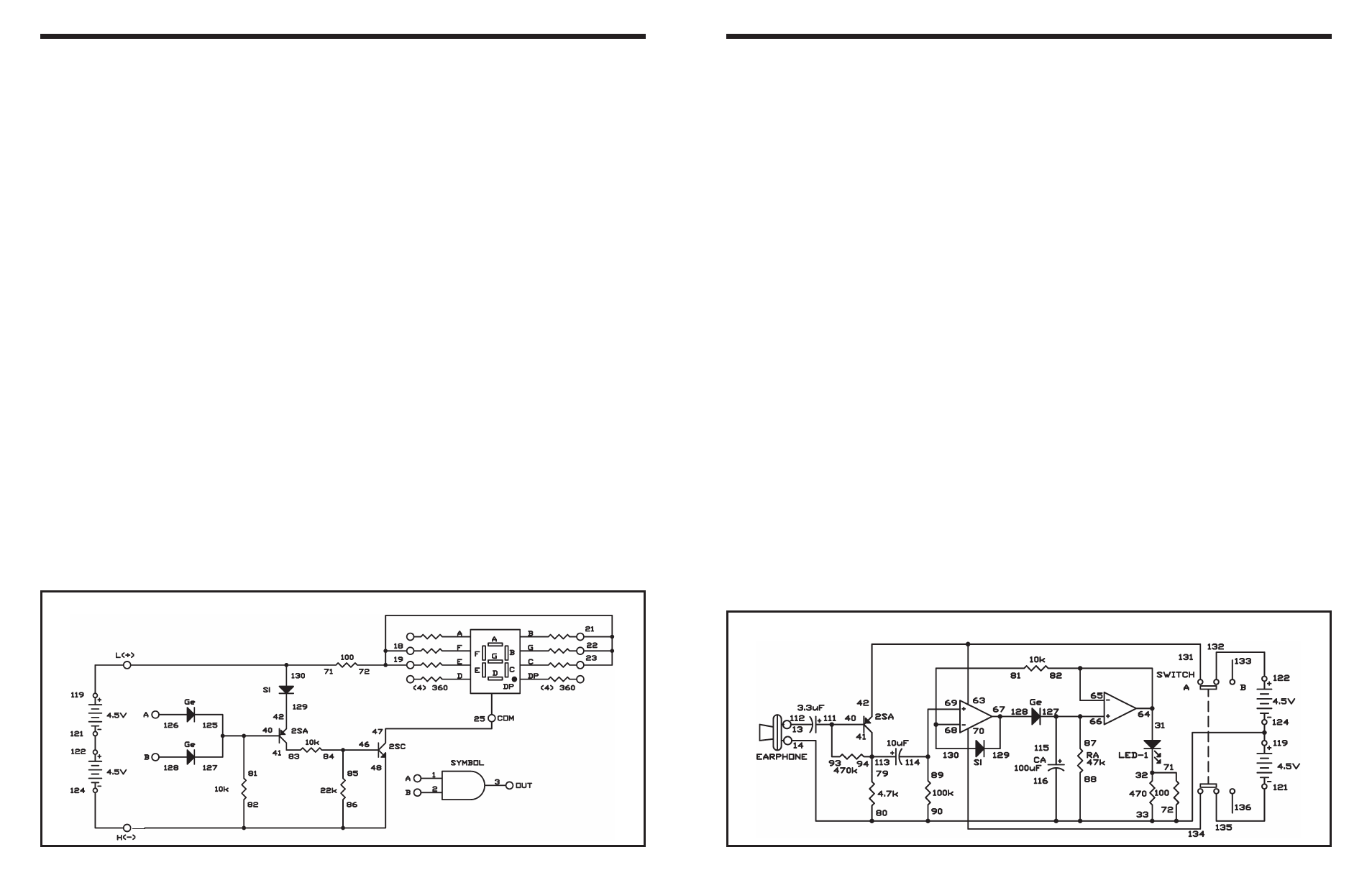
EXPERIMENT #29: “AND” DIODE TRANSISTOR LOGIC WITH LED DISPLAY
Wiring Sequence:
o 22-23-21-18-19-72
o 25-47
o 81-40-125-127
o 41-83
o 42-129
o 46-84-85
o 86-82-48-124
o 71-130-119
o 121-122
o 126-(to 119 “HIGH” or 124 “LOW”)
o 128-(to 119 “HIGH” or 124 “LOW”)
Schematic
In this experiment, you will create a voice input power
meter. The brightness of the LED in this circuit
changes according to the level of voice input that
comes from the microphone (the earphone). Since
voice levels change quickly, the brightness of the LED
should also adjust quickly. In order to show the
highest voice input levels, we use a circuit called a
peak-level hold circuit. This allows the LED to hold
certain brightness after it reaches peak strength,
rather than turning off immediately.
Build the circuit, and set the switch to position A. You
will use the earphone as a microphone. Speak loudly
or blow strongly into the earphone. You can see the
LED get brighter temporarily and then gradually grow
dimmer.
Study the schematic. You can see that the signal from
the earphone travels through the PNP transistor and
then becomes the positive (+) input for the first
operational amplifier. The output level of the first
operational amplifier is stored in the 100mF capacitor,
and slowly discharges through the 47k
Ω resistor. The
LED gets dim as the voltage on the capacitor
decreases. The voltage that lights the LED is also fed
back to the negative (-) input of the first operational
amplifier, where it is compared to the signal from the
earphone. If the signal from the earphone is larger, it
charges the 100mF capacitor; otherwise there is no
output from it.
You can modify the brightness of the LED by
changing resistor RA (47k
Ω) or the capacitor CA
(100
μF).
Notes:
EXPERIMENT #97: VOICE POWER METER
Wiring Sequence:
o 112-13-EARPHONE
o 119-124-116-33-88-90-80-72-14-EARPHONE
o 31-65-64-82
o 32-71
o 93-111-40
o 79-94-113-41
o 63-42-131
o 87-66-127-115
o 67-129-128
o 81-68-130
o 89-69-114
o 70-134
o 121-135
o 122-132
Schematic