72 dds frequency register daca – 0x1cc (write) – Sundance SMT712 User Manual
Page 75
User Manual SMT712
Page 75 of 89
Last Edited: 11/12/2012 10:36:00
4.6.1.1.72
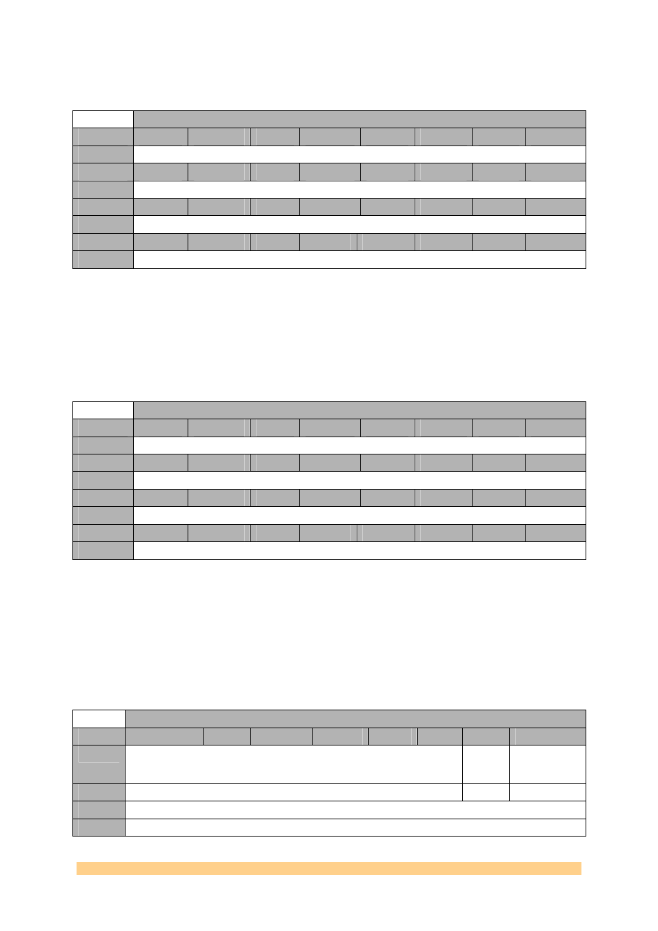
DDS Frequency Register DACA – 0x1CC (write).
DDS Frequency Register DACB – 0x1CC (write)
Byte
Bit 7
Bit 6
Bit 5
Bit 4
Bit 3
Bit 2
Bit 1
Bit 0
3
DDS Frequency Register[31:24]
Byte
Bit 7
Bit 6
Bit 5
Bit 4
Bit 3
Bit 2
Bit 1
Bit 0
2
DDS Frequency Register[23:16]
Byte
Bit 7
Bit 6
Bit 5
Bit 4
Bit 3
Bit 2
Bit 1
Bit 0
1
DDS Frequency Register[15:8]
Byte
Bit 7
Bit 6
Bit 5
Bit 4
Bit 3
Bit 2
Bit 1
Bit 0
0
DDS Frequency Register[7:0]
The FPGA implements a DDS block that takes a 32-bit word to set the frequency
(phase increment). Note that the phse increment should be an entire multiple of 8.
The maximum frequency that can be programmed is 0xFFFFFFF8, which
corresponds to 1/8
th
of the DAC sampling frequency.
The DDS output frequency is calculated as follows:
Fout = 0.125 * Phase Increment / 2
32
.
4.6.1.1.73
DDS Frequency Register DACB – 0x1D0 (write).
DDS Frequency Register DACB – 0x1D0 (write)
Byte
Bit 7
Bit 6
Bit 5
Bit 4
Bit 3
Bit 2
Bit 1
Bit 0
3
DDS Frequency Register[31:24]
Byte
Bit 7
Bit 6
Bit 5
Bit 4
Bit 3
Bit 2
Bit 1
Bit 0
2
DDS Frequency Register[23:16]
Byte
Bit 7
Bit 6
Bit 5
Bit 4
Bit 3
Bit 2
Bit 1
Bit 0
1
DDS Frequency Register[15:8]
Byte
Bit 7
Bit 6
Bit 5
Bit 4
Bit 3
Bit 2
Bit 1
Bit 0
0
DDS Frequency Register[7:0]
The FPGA implements a DDS block that takes a 32-bit word to set the frequency
(phase increment). Note that the phse increment should be an entire multiple of 8.
The maximum frequency that can be programmed is 0xFFFFFFF8, which
corresponds to 1/8
th
of the DAC sampling frequency.
The DDS output frequency is calculated as follows:
Fout = 0.125 * Phase Increment / 2
32
.
4.6.1.1.74
DACA DCM Phase Shifts – 0x1D4 (write).
Offset 0x0400 – DACA DCM Phase Shifts – 0x1D4 (write).
Byte
Bit 7
Bit 6
Bit 5
Bit 4
Bit 3
Bit 2
Bit 1
Bit 0
1
DACA DCM
Phase Shift
Sign
Default
‘0’
0
DACA DCM Phase Shift[7:0]
Default
‘00000000’