Sundance SMT712 User Manual
Page 20
User Manual SMT712
Page 20 of 89
Last Edited: 11/12/2012 10:36:00
F
s
/8
Fs
Fs
O
U
T
2
O
U
T
0
‘1
’
‘And’
Gate
‘And’
Gate
O
U
T
3
Flip
Flop
Sync
Pulse
F
s/
8
DAC A
S
a
m
p
le
s
DAC B
S
a
m
p
le
s
Virtex 5 LX110T-3
A
n
a
lo
g
O
u
t
B
A
n
a
lo
g
O
u
t
A
DCM
DACB
with
phase
shift
adjust.
DACB
reference
clock
Clock Mux
DCM
DACA
with
phase
shift
adjust.
DACA
reference
clock
Clock Mux
E
xt
e
rn
a
l
C
lo
ck
O
u
tp
u
t
Clock Distribution
AD9516-2
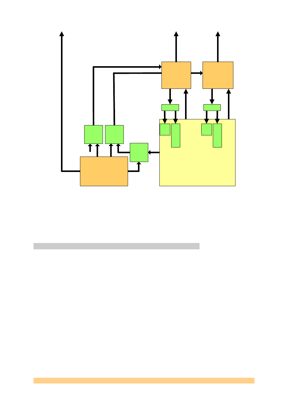
Figure 6 - SMT712 Clock circuitry.
On the FPGA side, one Xilinx DCM is implemented per channel. They are used to
clock the logic, to be able to change their phase shift to align outgoing data and
incoming clock. Both DCM are set in High Frequency Mode. This mode has a
limitation in terms of input clock (120 Mhz minimum), which implies a minimum
sampling frequency of 960 MSPS.
4.5.6
Data (samples) path / Data storage
This section details how samples can be routed to the DACs. By default and after
power-up or reset operation, all interfaces are in reset state. The only exception is
for the PXI/PXIe bus interface. Relevant interfaces should first be taken out of the
initial reset state.
The next step is to program both DACs and the clock generator and make sure it
locked to a reference signal. This is not needed in case of using an external
sampling clock. A DAC synchronisation cycle can be run to make sure their Fs/8
output clocks are in phase. DACs are then ready to receive samples and output a
clock to the FPGA.
Here are the details of the following step. One Xilinx DCM per DAC clock is used
inside the FPGA to ensure a good capture of data. The status of these DCMs should
be checked to make sure they are ‘locked’. They are available in the Global Control
Register. The DDR2 interface uses some Xilinx specific blocks, such as idelays,
DCMs and Phy, which have to be ‘locked’ and ‘ready’ as well. These have to be
checked the same way, using the bits available from the Global Control Register.