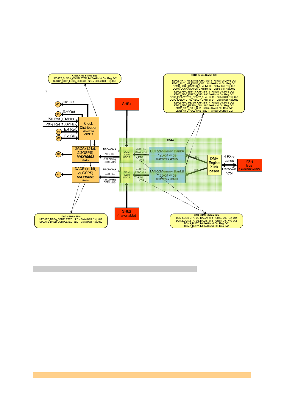
Figure 7 - data path – Sundance SMT712 User Manual
Page 21

User Manual SMT712
Page 21 of 89
Last Edited: 11/12/2012 10:36:00
Each DAC has a dedicated bank of DDR2 Memory, which can be seen as a Fifo. Both
Fifos have status bits to check whether they are empty or full (bit available from
Global Control Register). Each Fifo is connected to a DMA channel. DMA channel are
implemented as Xlinks. Each FIFO is used in the firmware as a pattern generator.
Once samples are written into it, the can be played out in a repetitive way, the size
of the pattern is loaded into a register.
The following diagram shows the data path implemented:
4
x8
b
its
(2
8
7
.5
M
H
z)
D
D
R
L
V
D
S
4
x
8
b
its
(2
8
7
.5
M
H
z
)
D
D
R
L
V
D
S
Figure 7 - Data path.
Note the data coming from the SHB are coming on 8 bits and casted to 12 bits to
match the DAC inputs.
4.5.7
PXI Express Bus
As standard, the SMT712 is a 3U PXI Express peripheral module, which means it
comes with two PXI Express connectors: XP4 (PXI timing and synchronisation
signals) and XP3 (x8 PCI Express and additional synchronisation signals). The
SMT712 dedicates 8 lanes to the PXI Express bus, which gives an effective
bandwidth per direction of 16Gb/s. It also implies core and user clocks to be 250
MHz. Note that not all PXIe Express chassis can handle 8 lanes on peripheral
modules. The default SMT712 firmware (For PXIe version of the board) only
implements 4 lanes.
The standard SMT712 can plug in any PXI Express Peripheral Slot or any PXI Express
Hybrid Slot.
