Sundance SMT712 User Manual
Page 13

User Manual SMT712
Page 13 of 89
Last Edited: 11/12/2012 10:36:00
4.4
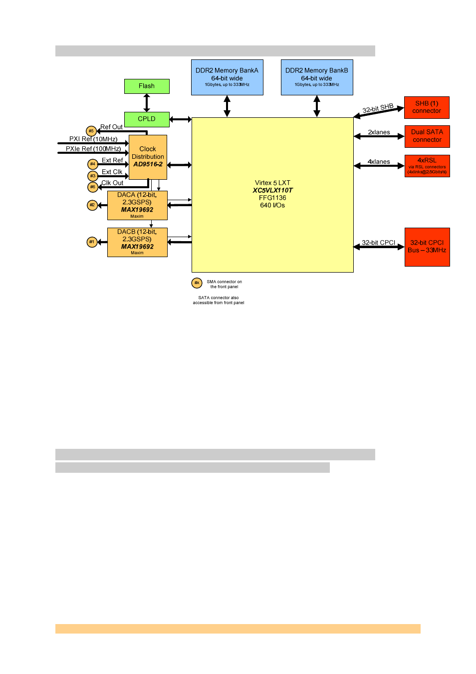
Block Diagram – SMT712-CPCI32 (Option 32-bit PCI)
Figure 4 - SMT712-CPCI32 Block Diagram (32-bit CPCI Option)
This option implements a 32-bit PCI core (33 Mhz). Note that PXI trigger signals and
reference clock (10Mhz) are not accessible by the PFGA (not available on a standard
CPCI rack). An external reference clock would have to be used.
The PCI core source core cannot be supplied by Sundance as the license held does
not cover such use for it.
The SMT712-CPCI32 can be plugged in either a PXI (CompactPCI) or PXI Express
rack.
Note that not all resources shown on the above diagram are implemented in the
standard firmware.
4.5
Module Description
4.5.1
DACs
The DACs are 12-bit parts from Maxim (MAX19692). On the SMT712, each DAC can
achieve up to 2.3 GSPS, via a built-in 4:1 multiplexer.
Both DACs have a selectable frequency response mode, that can be NRZ (Non-
Return-to-Zero – high dynamic range and output power in the first Nyquist zone),
RZ (Return-to-Zero – this mode trades off SNR for improved gain flatness in the
first, second and third Nyquist zones) or RF (Radio Frequency – high SNR and
dynamic range in the second and third Nyquist Zones). For more information, please
refer to the MAX19692 datasheet (Maxim).
The typical output power of the MAX19692 is -2.6 dBm (50-Ohm – Full scale). These
are the manufacturer figures.
Both DACs are AC coupled using RF transformers.
