Sundance SMT712 User Manual
Page 39
User Manual SMT712
Page 39 of 89
Last Edited: 11/12/2012 10:36:00
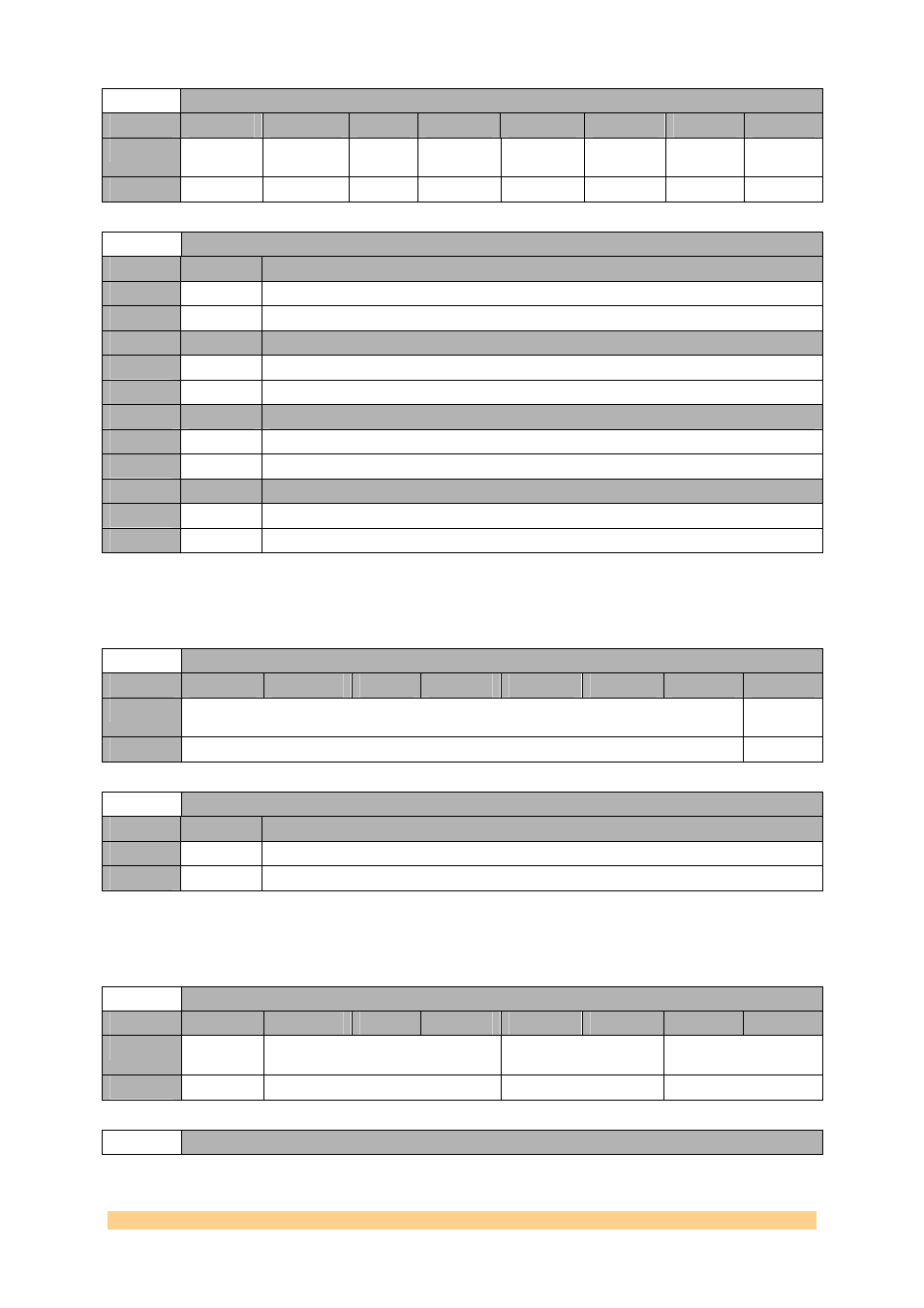
Clock Generator (AD9516-2) Register 0x00 – Serial Port Configuration – 0xC0 (write)
Byte
Bit 7
Bit 6
Bit 5
Bit 4
Bit 3
Bit 2
Bit 1
Bit 0
0
SDO
Active
LSB First
Soft
reset
Long
Instruction
Long
Instruction
Soft Reset
LSB First
SDO
Active
Default
‘0’
‘0’
‘0’
‘1’
‘1’
‘0’
‘0’
‘0’
Clock Generator (AD9516-2) Register 0x00 – Serial Port Configuration – 0xC0 (write)
Setting
Bit 3
Description (Long Instruction)
0
0
N/A
1
1
16-bit instruction (long).
Setting
Bit 2
Description (Soft Reset)
0
0
Must be cleared to '0' to complete reset operation.
1
1
'1' (not self-clearing). Soft reset
Setting
Bit 1
Description (LSB First)
0
0
data-oriented MSB first; addressing decrements.
1
1
data-oriented LSB first; addressing increments.
Setting
Bit 0
Description (SDO Active)
0
0
SDIO pin used for write and read; SDO set high impedance; bidirectional mode.
1
1
SDO used for read; SDIO used for write; unidirectional mode
4.6.1.1.7
Clock Generator (AD9516-2) Register 0x04 – Read-back
Control – 0XC4 (write).
Clock Generator (AD9516-2) Register 0x04 – Read-back Control – 0XC4 (write)
Byte
Bit 7
Bit 6
Bit 5
Bit 4
Bit 3
Bit 2
Bit 1
Bit 0
0
Reserved
Read-back
Active
Default
‘0000000’
‘0’
Clock Generator (AD9516-2) Register 0x04 – Read-back Control – 0XC4 (write)
Setting
Bit 0
Description (Read-back Active Registers)
0
0
read back buffer registers
1
1
read back active registers.
4.6.1.1.8
Clock Generator (AD9516-2) Register 0x10 – PFD and
Charge Pump – 0xC8 (write).
Clock Generator (AD9516-2) Register 0x10 – PFD and Charge Pump – 0xC8 (write)
Byte
Bit 7
Bit 6
Bit 5
Bit 4
Bit 3
Bit 2
Bit 1
Bit 0
0
PFD
Polarity
Charge Pump Current
Charge Pump Mode
PLL Power Down
Default
‘0’
‘111’
‘11’
‘11’
Clock Generator (AD9516-2) Register 0x10 – PFD and Charge Pump – 0xC8 (write)