6 fpga design – Sundance SMT712 User Manual
Page 28
User Manual SMT712
Page 28 of 89
Last Edited: 11/12/2012 10:36:00
4.6
FPGA Design
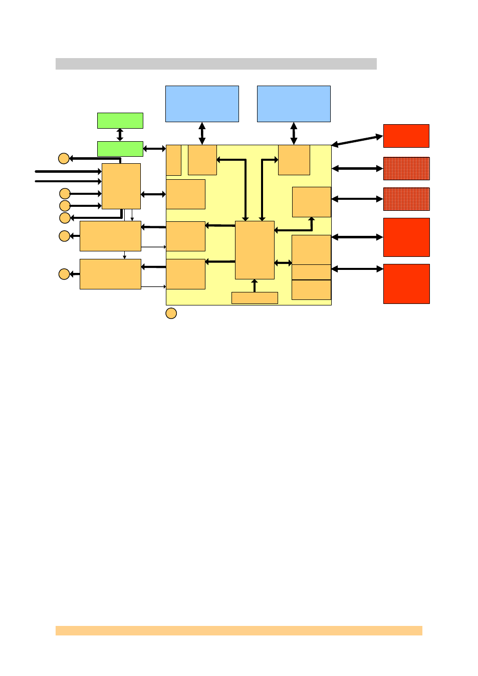
The following block diagram shows how the default FPGA design is organised.
Flash
DDR2 Memory BankA
64-bit wide
1Gbytes, 312MHz
CPLD
4x12
DDR
LVDS
4x12
DDR
LVDS
DDR2 Memory BankB
64-bit wide
1Gbytes, 312MHz
#2
#1
#3
Ext Clk
#4
Ext Ref
Clock
Distribution
AD9516-2
Virtex 5 LXT
4x12 bits
(287.5 MHz)
DDR
LVDS
4x12 bits
(287.5 MHz)
DDR
LVDS
DDR2
Interface
Pattern
Generator
RSL
Interface
4
x
1
2
b
it
s
(
2
8
7
.5
M
H
z
)
D
D
R
L
V
D
S
4
x
1
2
b
it
s
(
2
8
7
.5
M
H
z
)
D
D
R
L
V
D
S
Clock SPIs
Data
Router and
FIFOs
#x
SMA connector on
the front panel
2xlanes
Dual SATA
connector
(optional)
4 PXIe Lanes
Data&Control
PXIe
Bus on PXIe
version
4xlanes
4xRSL
via RSL connectors
(optional)
32-bit PXI/CPCI
32-bit on PXI/
CPCI versions
Otherwise
SHB (2)
PCI
Express
Core
Control
Registers
PCI Interface
PXIe Ref (100MHz)
PXI Ref (10MHz)
#5
Ref Out
#6
Clk Out
SHB
connector
32-bit
SHB
DDSA and B
2 Clocks
287.5Mhz
2 Clocks
287.5mhz
DDR LVDS
IOs
DDR LVDS
IOs
DACB (12-bit,
2.3GSPS)
MAX19692
Maxim
DACA (12-bit,
2.3GSPS)
MAX19692
Maxim
DDR2
Interface
Pattern
Generator
CPLD
Inter
face
Figure 14 - Block Diagram - FPGA Design (standard Firmware).
The FPGA implements some control registers in order to configure and control all
blocks. Most of them are available to read-back.
DDR2 interfaces have been designed in such way that both banks can be used as a
pattern generator. Each memory interface uses some Xilinx specific blocks such as
IDelay and DCM. Their respective status Ready and Lock are available from the
Control Register. A pattern can be stored on the DDR2 memory and played back.
A 32-bit SHB (1) connector is available. A second one is shared with the PCI 32-bit
bus, i.e. you can have one or the other depending on the option ordered.
DACs provide the FPGA with with a divided version of the sampling clock (sampling
clock/8). DCMs are used so they can be phase-adjusted. DCMs Status is available
from the Control Register. DCMs introduces a limitation of the sampling clock
(DCMs won’t work when sampling clocks are below 960MHz).
The PCI Express interface (when option purchased) implements 4 Express lanes.
The PCI 32-bit (33Mhz) (when option purchased) implements some Xilinx specific
blocks such as IDelays and DCMs. Status bits are available from the Control
Register. On non-PCI versions of the board a second 32-bit SHB (2) connector is
fitted.
The FPGA is also responsible for accesses to the CPLD in order to access the flash
memory that can contain up to 4 bitstreams. The CPLD can be triggered to reload
the FPGA with a different bistream. In this situation, the Sundance driver (SMT6300)
ensures that the link between the host application and the board is not lost.