Flash cpld, Fpga, Switch – Sundance SMT712 User Manual
Page 17

User Manual SMT712
Page 17 of 89
Last Edited: 11/12/2012 10:36:00
Number of SYSMONs: 1 out of 1 100%
Number of RPM macros: 128
Average Fanout of Non-Clock Nets: 3.36
The part mentioned above is also footprint compatible with the SXT series:
XC5VSX50T and XC5VSX95T. The SXT series implements a DSP48E core, which if
used on the SMT712 may result an increase of the power consumption. Please
contact Sundance if you require details about the SXT series.
4.5.3
Configuration (CPLD+Flash)
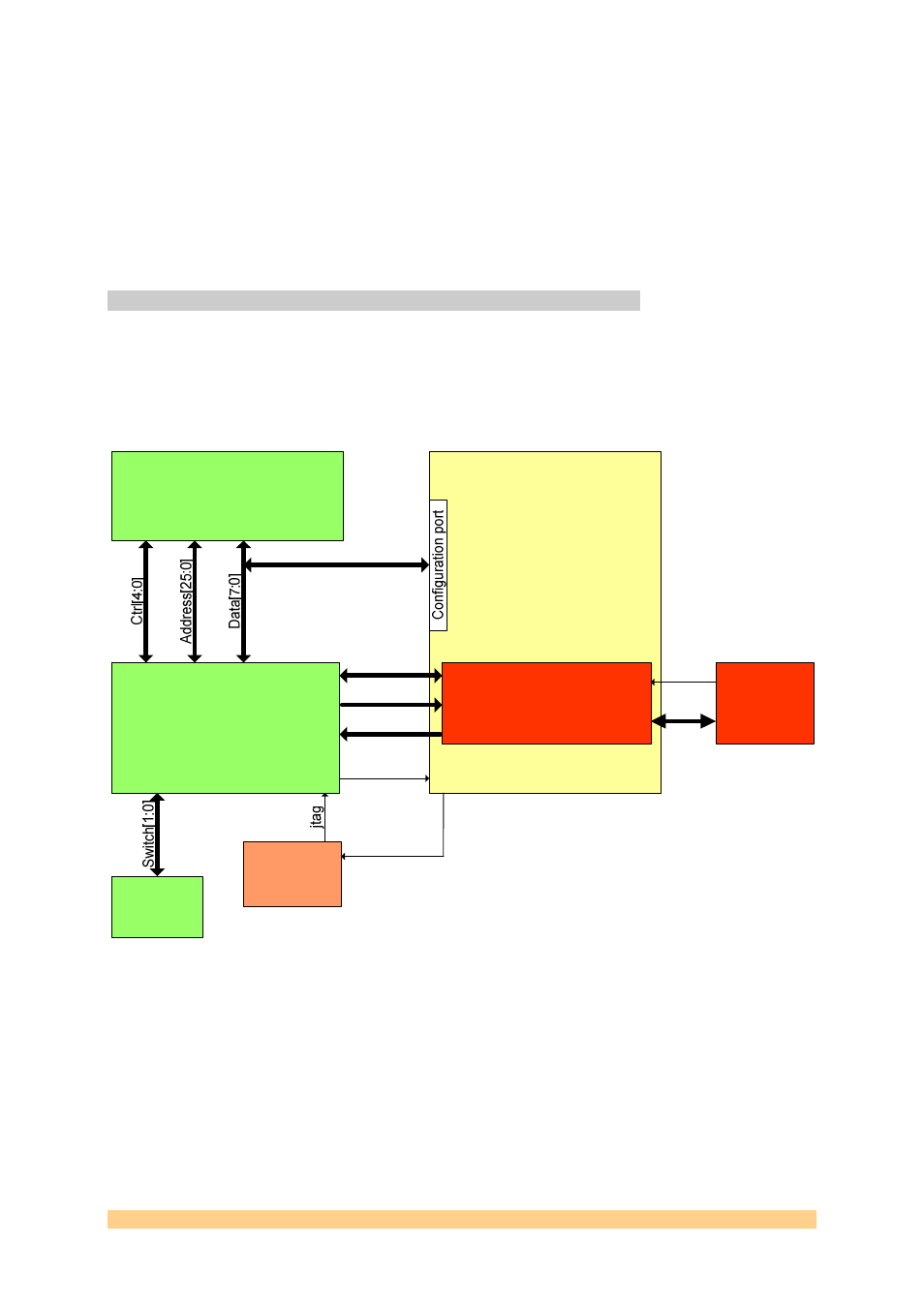
On the SMT712, the FPGA is connected to a CPLD via a serial link. The CPLD is
responsible for controlling read and write operations to and from the Flash memory
and to route data to the FPGA configuration port.
The following diagram show how connections are made on the board between the
CPLD, the Flash memory and the FPGA:
Data[7:0]
Flash
CPLD
PXIe
Bus or 32-bit
PCI Bus
FPGA
Ctrl[9:0]
JTAG
Connector
(J8)
jtag
Jtag
Configuration Task
Serial Link
Serial Link
Reset
Switch
(bitstream
selection)
Figure 5 - Configuration (Flash).
A reset coming from the bus (PXI/PCI or PXI Express) triggers a configuration cycle
and the FPGA is configured with the default firmware (stored in factory at location
0).
The on-board Flash memory (256-Mbit part) is big enough to store several versions
(4 in total on the SMT712) of firmware. A switch (SW1) at the back of the board
allows the selection among the 4 locations. It selects the bitstream to be loaded at
power up (only switches 1 and 2 of SW1 are used. Each can contain up to 8Mbytes of
