Figure 6-1, Glue logic fpga block diagram, Programmable logic – Artesyn ATCA-8330 Installation and Use (April 2015) User Manual
Page 128
Programmable Logic
ATCA-8330 Installation and Use (6806800S82B)
128
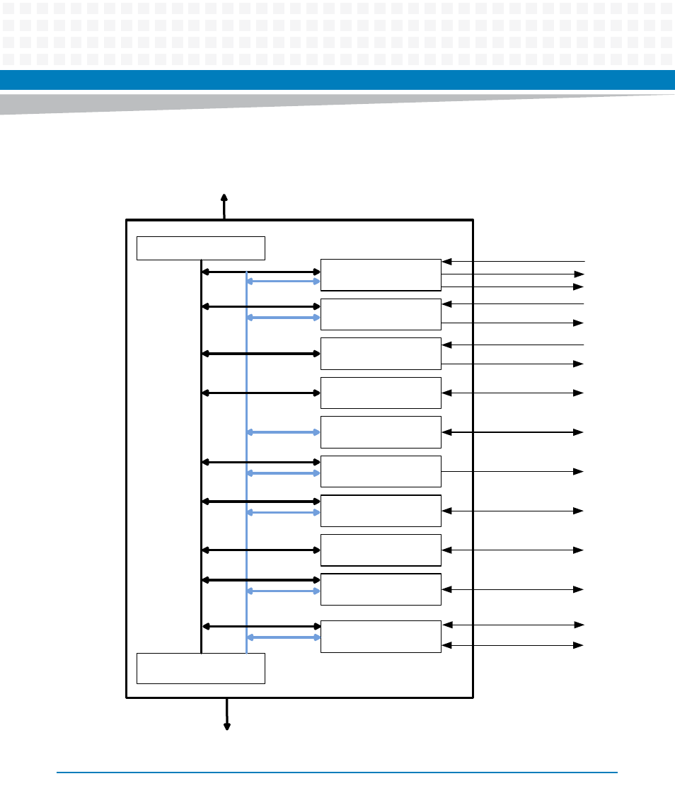
The following block diagram shows the functional units inside the Glue Logic FPGA:
Figure 6-1
Glue Logic FPGA Block Diagram
LPC BUS Interface
Serial Line
Routing
Reset
Interrupt Routing
DSP SPI Master
DSP I2C Master
Post Code
Register
SPI Flash Control
Status
DSP Power
Control
Several
Control/Status
DSP/CPLD FPGA
Update Register
IPMC SPI
Interface
Serial Interfaces
Serial Signals
Serial Signals
RST_IN
RST_OUT
INT_IN
INT_OUT
DSP SPI Interface
DSP I2C Interface
7 Segment LED Displays
SPI Flash Control Signals
DSP Power Status/Control
Several Board Control/
Status Signals
DPS FPGA JTAG
Power-up CPLD JTAG
LPC Bus
IPMC SPI
See also other documents in the category Artesyn Equipment:
- ARTM-9405 16x10GbE Installation and Use Guide (May 2014) (64 pages)
- ATCA 7370 / ATCA 7370-S Installation and Use (January 2015) (256 pages)
- ATCA 7370 / ATCA 7370-S Installation and Use (September 2014) (254 pages)
- ARTM-831X Installation and Use (June 2014) (346 pages)
- ATCA-7350 - Integrating with Workbench User Guide (September 2014) (34 pages)
- ATCA-7350 Installation and Use (September 2014) (208 pages)
- ATCA-7365-CE Installation and Use (May 2014) (306 pages)
- ATCA-7365-CE Installation and Use (Jan 2015) (300 pages)
- ATCA-7365-CE Installation and Use (May 2014) (294 pages)
- ATCA-7368 Installation and Use (June 2014) (222 pages)
- ATCA-7475 Installation and Use (October 2014) (284 pages)
- ATCA-7480 Installation and Use (April 2015) (330 pages)
- ATCA-8320 Installation and Use (May 2014) (456 pages)
- ATCA-9305 User's Manual (May 2014) (270 pages)
- ATCA-9405 Installation and Use (October 2014) (168 pages)
- ATCA-F120 Installation and Use (August 2014) (122 pages)
- ATCA-F140 Installation and Use (September 2014) (138 pages)
- ATCA-MF106 Installation and Use (September 2014) (86 pages)
- Centellis-4440/AXP1440 Installation and Use (September 2014) (208 pages)
- Centellis 4410 (AXP-1410) Installation and Use (July 2014) (202 pages)
- Centellis 2100 Release 3.0 Installation and Use (March 2015) (192 pages)
- Centellis 2100 Release 3.0 Installation and Use (March 2015) (176 pages)
- Centellis 2000 User Card-10GE Installation and Use (May 2014) (54 pages)
- Centellis 2000 User Card-10GE with Telco Alarm Installation and Use (May 2014) (60 pages)
- COMX-CAR-210 Installation and Use (August 2014) (76 pages)
- COMX-P1022 Installation and Use (July 2014) (84 pages)
- COMX-P2020 Installation and Use (February 2015) (100 pages)
- COMX-CORE Series Installation and Use (August 2014) (128 pages)
- COMX-P2020 Installation and Use (July 2014) (100 pages)
- COMX-P4080-2G-ENP2 Installation and Use (August 2014) (70 pages)
- COMX-P4080 Installation and Use (August 2014) (126 pages)
- COMX-P40x0 ENP2 Installation and Use (August 2014) (130 pages)
- COMX-P40x0 ENP2 Installation and Use (January 2015) (140 pages)
- iVPX7225 RTM Installation and Use (April 2015) (56 pages)
- MITX-430/MITX-440-DVI-2E Installation and Use (August 2014) (118 pages)
- CPCI-6200 Installation and Use (May 2015) (234 pages)
- SCP-MITX-CORE-820-SM Installation and Use (August 2014) (132 pages)
- iVPX7225 Installation and Use (April 2015) (168 pages)
- MVME2502 Installation and Use (August 2014) (150 pages)
- MVME2502 Installation and Use (December 2014) (166 pages)
- MVME2500 VxWorks 6.8 AMP User Guide (August 2014) (40 pages)
- MVME2500 VxWorks 6.8 User Guide (April 2014) (44 pages)
- MVME3100 Single Board Computer Installation and Use (June 2014) (156 pages)
- MVME4100 Single Board Computer Installation and Use (June 2014) (136 pages)