Altera RLDRAM II Controller MegaCore Function User Manual
Page 35
Altera Corporation
MegaCore Version 9.1
2–25
November 2009
RLDRAM II Controller MegaCore Function User Guide
Functional Description
shows the local interface signals.
reset_read_clk_n[]
DQS mode:
the number of
RLDRAM II devices
attached to the memory
interface
Non-DQS mode:
1
Input
Reset input for logic on the capture clock
domain. In DQS mode, the capture clock
domain is
capture_clk[]
; in non-DQS
mode, it is
non_dqs_capture_clk
. In
DQS mode, each
reset_read_clk_n[]
is associated
with the corresponding
capture_clk[]
clock domain. The
reset_read_clk_n[]
can be asserted
asynchronously but must be deasserted
synchronous to the rising edge of the
capture clock.
capture_clk[]
The number of
RLDRAM II devices
attached to memory
interface
Output
Undelayed DQS clock used by capture
circuitry to capture RLDRAM II read data.
There is one
capture_clk[]
per
attached RLDRAM II device. DQS mode
only.
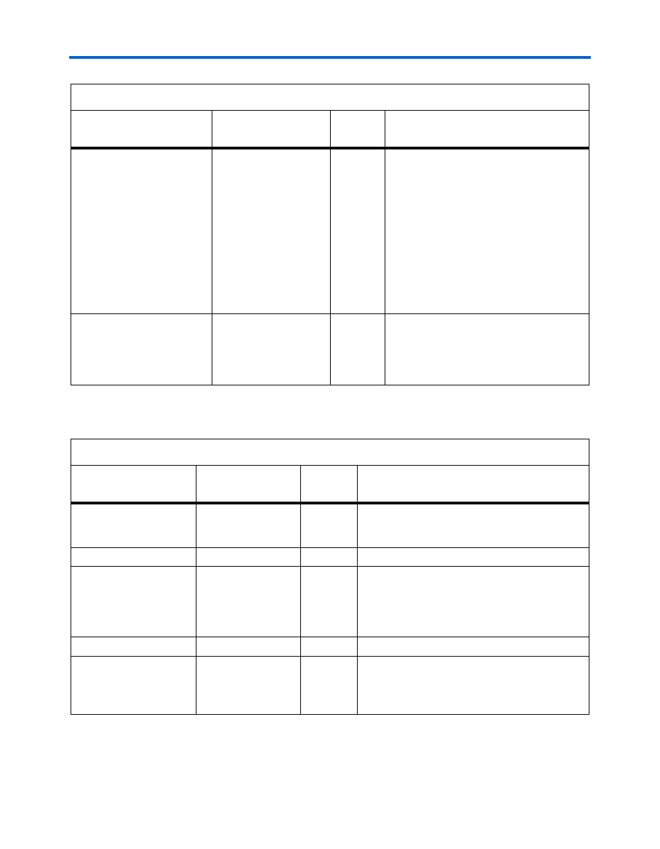
Table 2–3. System Signals (Part 3 of 3)
Name
Width
(Bits)
Direction
Description
Table 2–4. Local Interface Signals (Part 1 of 2)
Name
Width
(Bits)
Direction
Description
local_addr[]
Device dependant
Input
RLDRAM II address. IP Toolbench refers to the
memory.dat file and selects the address width
appropriate to the device.
local_bank_addr[]
3
–
RLDRAM II bank address.
local_dm[]
The number of
RLDRAM II devices
attached to the
memory interface ×
2
Input
Optional local data mask (DM). Twice the width of
the memory
rldramii_dm[]
bus. When all
high, all writes are masked.
local_read_req
1
Input
Read request signal.
local_refresh_req
1
Input
User controlled refresh request. This allows
complete control over when refreshes are issued
to the memory. The refresh is issued to the bank
address on
local_bank_addr[]
.