Example design, Figure 2–9. pll configuration – Altera RLDRAM II Controller MegaCore Function User Manual
Page 24
2–14
MegaCore Version 9.1
Altera Corporation
RLDRAM II Controller MegaCore Function User Guide
November 2009
Device-Level Configuration
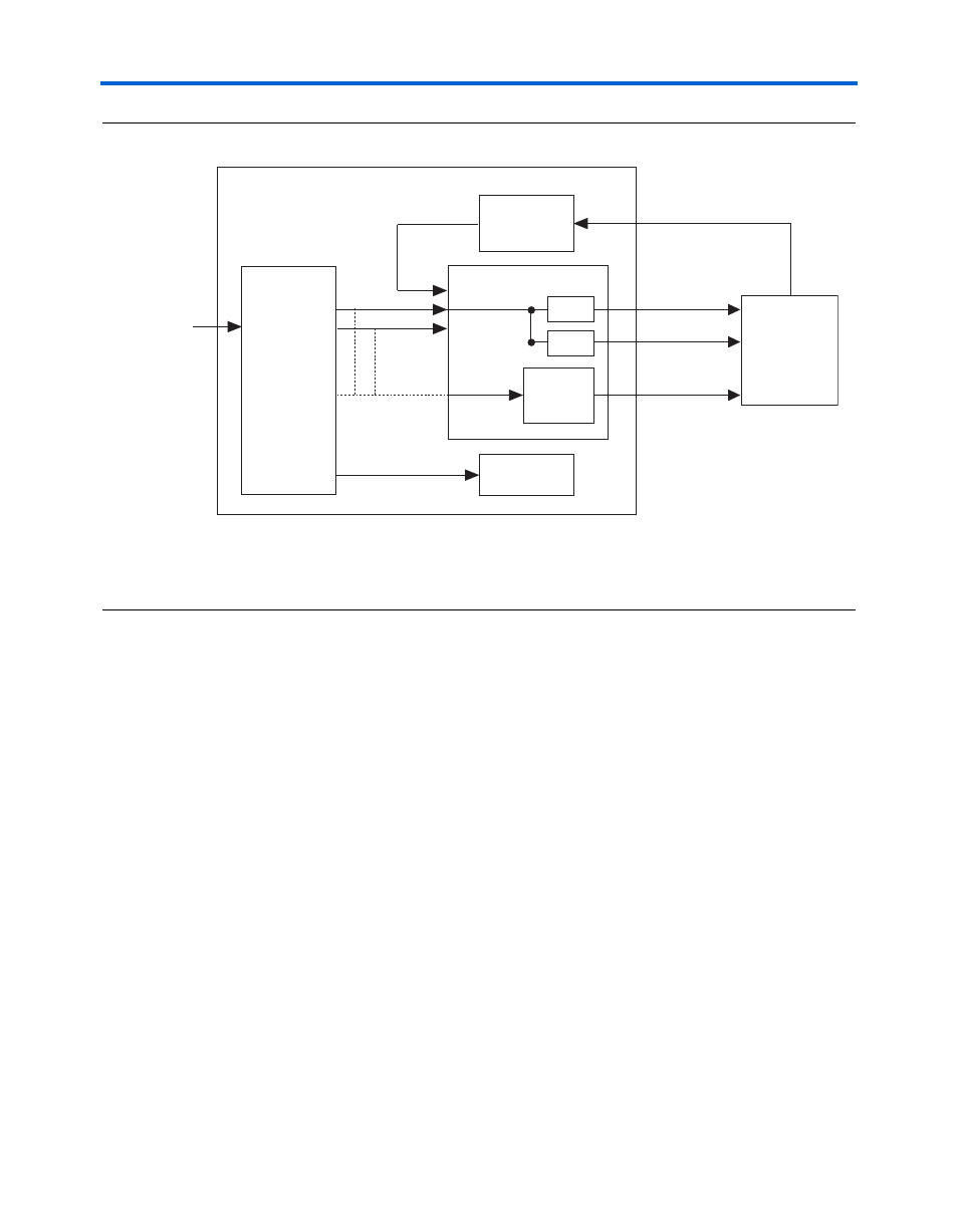
Figure 2–9. PLL Configuration
Notes to
(1)
Non-DQS mode only.
(2)
You can connect the addr_cmd_clk RLDRAM II controller input to clk, write_clk or to the dedicated PLL
output C2.
Example Design
IP Toolbench creates an example design that shows you how to
instantiate and connect up the RLDRAM II controller to an example
driver. The example design is a working system that can be compiled and
used for both static timing checks and board tests. It also instantiates an
example PLL that generates all the required clocks for the controller. In
DQS mode, a DLL is instantiated that controls the DQS capture delay
phase. In non-DQS mode, the example design instantiates a fedback PLL.
The output of the fedback PLL is a phase-shifted rldramii_qk[] data
strobe, which captures the read data.
The example driver is a self-checking test generator for the RLDRAM II
controller. It uses a state machine to write data patterns to all memory
banks. It then reads back the data and checks that the data matches. If any
read data fails the comparison, the pnf_per_byte output transitions
low for one cycle and the pnf_persist permanent output transitions
low and stays low.
shows a testbench and an example design.
Optional
Fed-Back Clock
PLL (Note 1)
FPGA Device
RLDRAM II
rldramii_clk_n
rldramii_clk
rldramii_a_0[]
rldramii_ba_0[]
rldramii_cs_n_0
rldramii_ref_n_0
rldramii_we_n_0
rldramii_qk
RLDRAM II Controller
altddio
clock_source
Enhanced PLL
clk
write_clk
non_dqs_capture_clk
addr_cmd_clk
(Note 2)
C0
C1
C2
C3
Stratix II DLL
altddio
Address &
Command
Registers