Memory clock generator, Address & command output registers – Altera RLDRAM II Controller MegaCore Function User Manual
Page 15
Altera Corporation
MegaCore Version 9.1
2–5
November 2009
RLDRAM II Controller MegaCore Function User Guide
Functional Description
■
Generates the RLDRAM II clocks
■
Generates addresses and commands on:
●
System, dedicated, or write clock
●
Rising or falling edge
■
Inserts pipeline registers in address and command and write data
path
■
Inserts pipeline registers in read data and QVLD path
The datapath provides the interface between the read and write data
busses of the datapath interface and the double-clocked, bidirectional
data bus of the memory interface. The datapath data busses are twice the
width of the memory data bus, because the memory interface transfers
data on both the rising and falling edges of the clock.
IP Toolbench generates a clear-text VHDL or Verilog HDL datapath,
which matches your custom variation. If you are designing your own
controller, Altera recommends that you use this module as your
datapath.
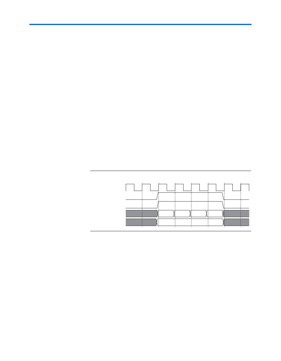
shows the write control signals timing relationship when
writing to the datapath.
Figure 2–3. Datapath Write Control Signal Timing
Memory Clock Generator
The memory clock generator generates memory clocks. There can be up
to four memory clocks and they are generated with an altddio_out
megafunction.
Address & Command Output Registers
The address and command output registers can have the following
options:
■
System, write, or dedicated clock clocking for the output registers.
■
Rising or falling edge clocking
clk
control_doing_wr
control_wdata_valid
control_wdata[]
control_dm[]
01
23
45
67
67
11
11