Of six-clock cycles (configuration two) – Altera RLDRAM II Controller MegaCore Function User Manual
Page 30
2–20
MegaCore Version 9.1
Altera Corporation
RLDRAM II Controller MegaCore Function User Guide
November 2009
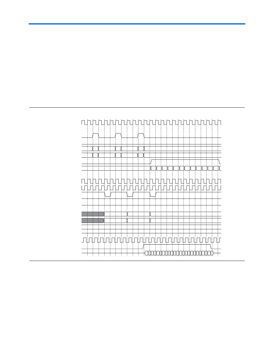
Interfaces
During reads, the local interface indicates that read data is valid by
asserting the local_rdata_valid[] signal. All captured read data is
clocked off the clock that captures the RLDRAM II read data. In DQS
mode, this clock is the delayed DQS signal, capture_clk[], sourced
from the dedicated DQS delay circuitry. In non-DQS mode this clock is
the external capture clock, non_dqs_capture_clk.
shows an example of a read at an SIO RLDRAM II interface.
In this example, the memory burst length is set to eight beats. The
RLDRAM II device is setup with a t
RC
of six-clock cycles (configuration
two).
Figure 2–14. Read Example
shows an example of a read following a write at a CIO
RLDRAM II interface. In this example, the memory burst length is set to
eight beats. The RLDRAM II device is setup with a t
RC
of six-clock cycles
(configuration two).
f
For more information about bus turnaround timing calculations with
CIO devices, refer to AN 325: Interfacing RLDRAM II with Stratix II,
Stratix & Stratix GX Devices.
clk
Local Interface
local_read_req
local_write_req
local_addr[]
local_bank_addr[]
local_rdata_valid[]
local_rdata[]
RLDRAM II Interface
rldramii_clk
rldramii_clk_n
rldramii_cs_n
rldramii_we_n
rldramii_ref_n
rldramii_a[]
rldramii_ba[]
rldramii_dm[ ]
rldramii_d[]
rldramii_qk[]
rldramii_qvld[]
rldramii_q[]
A
B
C
C
A
B
C
C
A01 A23 A45 A67 B01 B23 B45 B67 C01 C23C45 C67
C67
A
B
C
B
A
B
C
B
11
0 1 2 3 4 5 6 7 0 1 2 3 4 5 6 7 0 1 2 3 4 5 6 7
7