Datapath example, Dqs mode – Altera RLDRAM II Controller MegaCore Function User Manual
Page 18
2–8
MegaCore Version 9.1
Altera Corporation
RLDRAM II Controller MegaCore Function User Guide
November 2009
Block Description
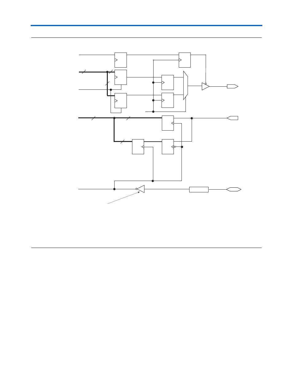
Figure 2–5. DQS Group Block Diagram—DQS Mode, SIO Devices
Notes to
(1)
This figure shows the logic for one Q output and one D input only.
(2)
All clocks are clk, unless marked otherwise.
(3)
Bus width W is dependent on the Q per DQS parameter.
(4)
Invert combout of the I/O element (IOE) for the dqs pin before feeding in to inclock of the IOE for the Q pin.
This inversion is automatic if you use an altdq megafunction for the Q pins.
Datapath Example
shows an example datapath. The example RLDRAM II
controller and memory configuration has the following parameters:
■
DQS mode
■
Two 18-bit CIO RLDRAM II devices. Each RLDRAM II device has
two rldramii_qk[] data strobes, each associated with 9-bits of
data
■
36-bit RLDRAM II interface, which requires a 72-bit datapath
interface
DQS
DQS Delay
Q
D
Q
D
Q
D
D
Q
Q
Q
D
Q
D
D
Q
D
Q
control_wdata
D
Q
write_clk
control_doing_wr
control_rdata
dq_capture_clk
dq_oe
0
1
2W
2W
W
D
EN
EN
control_wdata_valid
capture_clk
Note 4
W
W
W