NEC PD754144 User Manual
Page 53
CHAPTER 3 FEATURES OF ARCHITECTURE AND MEMORY MAP
53
User’s Manual U10676EJ3V0UM
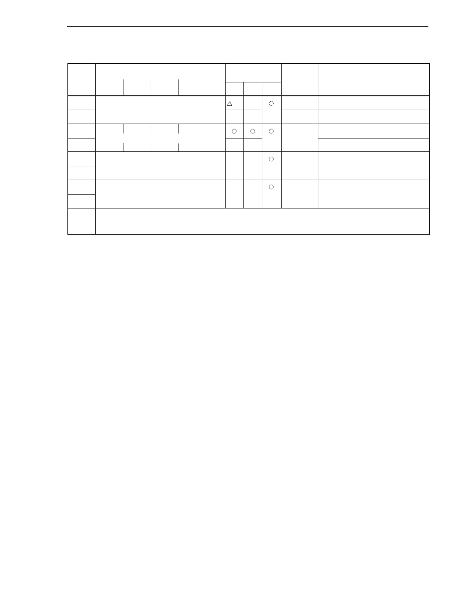
Figure 3-7.
µPD754244 I/O Map (2/8)
Hardware name (symbol)
Number of bits that
Bit
Address
R/W
can be manipulated
manipulation
Remarks
b3
b2
b1
b0
1-bit
4-bit
8-bit
addressing
F90H
Timer counter 2 mode register (TM2)
R/W
(W)
–
–
Bit manipulation can be performed only on bit 3
–
–
–
F92H
TOE2
REMC
NRZB
NRZ
R/W
–
Bit 3 can only be written
Timer counter 2 control register (TC2)
0
–
–
–
–
–
Only 0 can be written to bit 3
F94H
Timer counter 2 count register (T2)
R
–
–
–
F96H
Timer counter 2 modulo register (TMOD2)
R/W
–
–
–
F98H
Unmounted
to
F9FH
................................................................................
................................................................................
This manual is related to the following products: