3 pin i/o circuits – NEC PD754144 User Manual
Page 30
CHAPTER 2 PIN FUNCTIONS
30
User’s Manual U10676EJ3V0UM
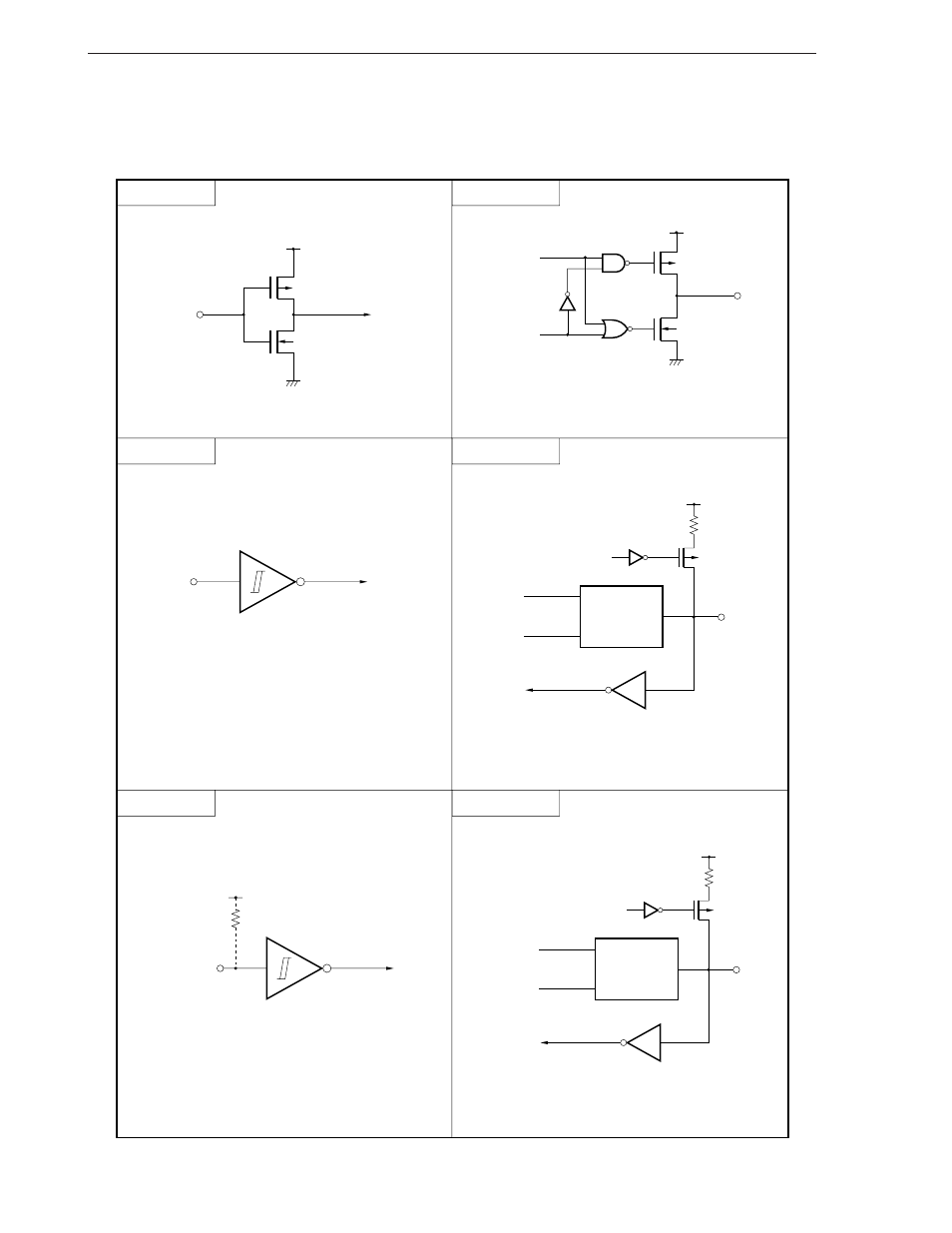
2.3 Pin I/O Circuits
The following diagrams show the I/O circuits of the pins of the
µPD754244. Note that in these diagrams the I/
O circuits have been slightly simplified.
Type A
Type B
Type D
Type E-B
Type B-A
Type F-A
V
DD
IN
P-ch
N-ch
Data
Output
disable
N-ch
P-ch
IN
OUT
V
DD
P-ch
Output
disable
Data
P.U.R.
enable
Type D
Type A
IN/OUT
V
DD
P.U.R (Mask Option)
IN
V
DD
P.U.R.
P.U.R.
enable
P-ch
IN/OUT
Type D
Type B
Output
disable
Data
P.U.R. : Pull-Up Resistor
P.U.R. : Pull-Up Resistor
P.U.R. : Pull-Up Resistor
Schmitt-triggered input with hysteresis characteristics.
CMOS specification input buffer.
Push-pull output that can be placed in output
high-impedance (both P-ch, N-ch off).
P.U.R.
V
DD
This manual is related to the following products: