4 block diagram – NEC PD754144 User Manual
Page 20
CHAPTER 1 GENERAL
20
User’s Manual U10676EJ3V0UM
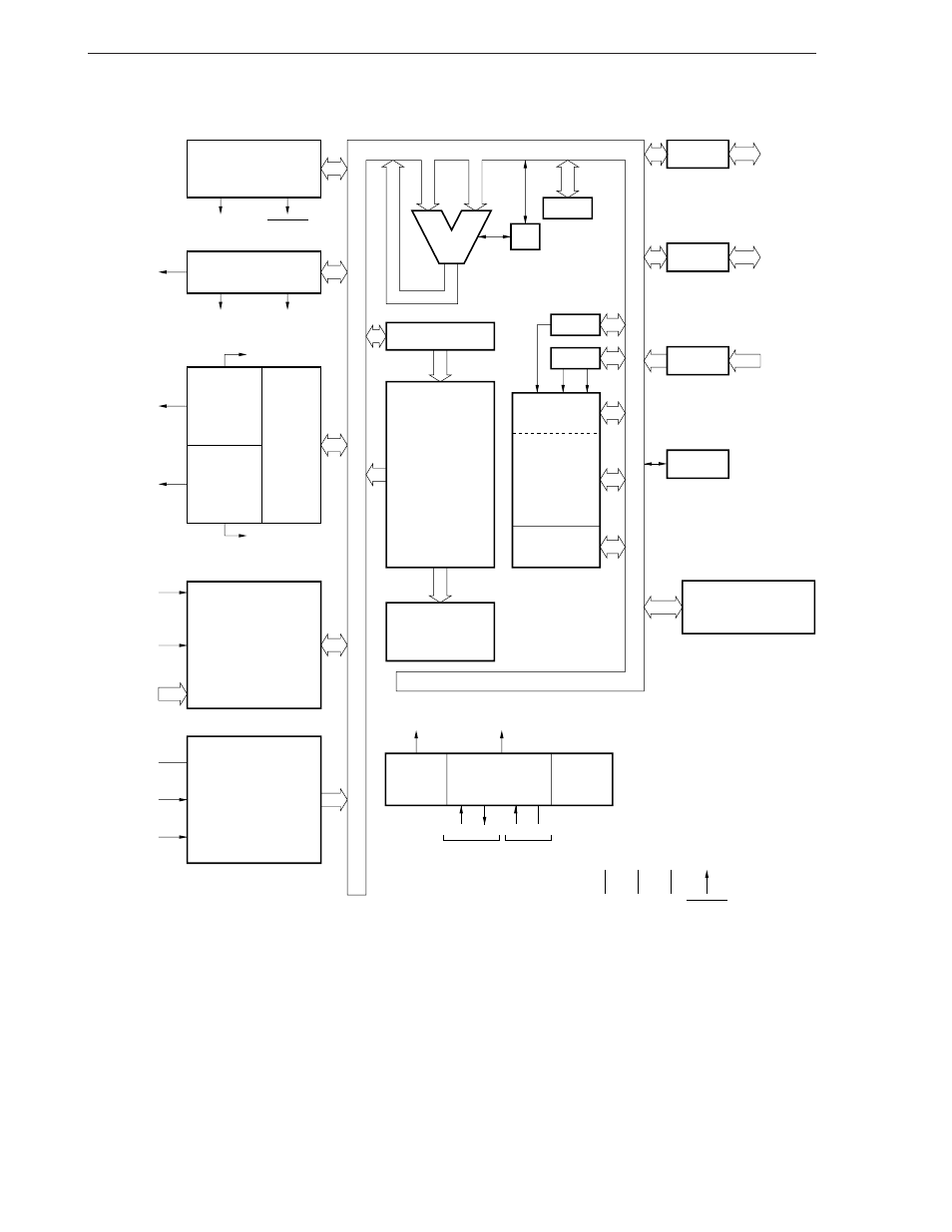
1.4 Block Diagram
Basic interval
timer/watchdog timer
8-bit timer counter #0
8-bit timer
counter #1
8-bit timer
counter #2
Cascaded
16-bit
timer
counter
Interrupt control
Programmable
threshold port
INTBT
RESET
INTT0
TOUT
INTT1
INTT2
PTO0/P30
PTO1/P31
PTO2/P32
INT0/P61
KRREN
KR4/P70-
KR7/P73
AV
REF
/P60
PTH00/P62
PTH01/P63
ALU
Program counter
Program memory
(ROM)
4096
× 8 bits
Decode and
control
CY
SP (8)
SBS
Bank
General reg.
Data memory
(RAM)
128
× 4 bits
EEPROM
16
× 8 bits
Port 3
4
Port 6
4
Port 7
4
Port 8
Bit seq. buffer (16)
P30 to P33
P60 to P63
P70 to P73
P80
Clock
divider
System clock
generator
Standby
control
f
X
/2
N
φ
CPU clock
IC
V
DD
V
SS
RESET
4
In the case of
PD754144
µ
In the case of
PD754244
µ
CL1 CL2 X1
X2
This manual is related to the following products: