NEC PD754144 User Manual
Page 52

CHAPTER 3 FEATURES OF ARCHITECTURE AND MEMORY MAP
52
User’s Manual U10676EJ3V0UM
................................................................................
................................................................................
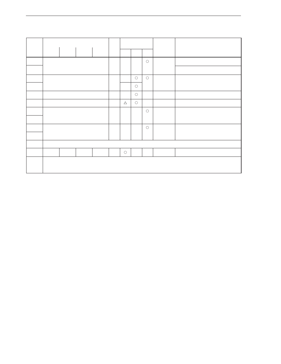
Figure 3-7.
µPD754244 I/O Map (1/8)
Hardware name (symbol)
Number of bits that
Bit
Address
R/W
can be manipulated
manipulation
Remarks
b3
b2
b1
b0
1-bit
4-bit
8-bit
addressing
F80H
Stack pointer (SP)
R/W
–
–
–
Bit 0 is fixed to 0.
F82H
Register bank selection register (RBS)
–
–
Note 1
Bank selection register (BS)
R
F83H
Memory bank selection register (MBS)
–
F84H
Stack bank selection register (SBS)
R/W
–
–
–
F85H
Basic interval timer mode register (BTM)
W
–
mem.bit
Bit manipulation can be performed only on bit 3.
F86H
Basic interval timer (BT)
R
–
–
–
F88H
Modulo register for setting timer counter 2
R/W
–
–
–
high-level period (TMOD2H)
F8AH
Unmounted
F8BH
WDTM
Note 2
–
–
–
W
–
–
mem.bit
F8CH
Unmounted
to
F8FH
Notes 1.
Manipulation is possible separately with RBS and MBS in 4-bit manipulation. Manipulation is possible
with BS in 8-bit manipulation. Write data into MBS and RBS with the SEL MBn (n = 0, 4 or 15) and
SEL RBn (n = 0-3) instructions.
2.
WDTM: Watchdog timer enable flag (W); Once set, cannot be cleared by an instruction.
