Logic scheme modification, Programmable logic decs-400, Figure 119. logic scheme modification illustration – Basler Electric DECS-400 User Manual
Page 196
184
9369700990 Rev R
Logic Scheme Modification
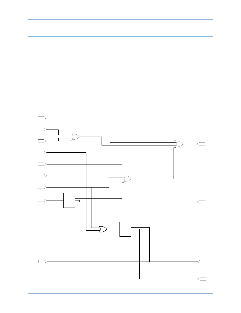
If desired, a predefined logic scheme can be altered to accommodate the specific needs of an application.
Logic scheme modification consists of the deletion and addition of logic components and connections to
achieve the desired logic functionality. Logic scheme modification is illustrated here through an example
where the “Single DECS-400 Without PSS” predefined logic scheme (illustrated in Figures 110, 110, and
111) is altered as shown in Figure 119. Figure 119 illustrates the portion of the “Single DECS-400 Without
PSS” logic scheme that will be modified. In Figure 119, an “X” indicates the deletion of a logic connection.
Bold lines indicate added components and connections. These changes are summarized as follows:
•
Buildup Active input buffer is disconnected from Output Relay #5
•
V/Hz Protection Active input buffer is disconnected from the Common Protection output (Relay
Output #2)
•
Field Overcurrent Active input buffer is disconnected from Relay Output #2
•
The V/Hz Protection Active and Field Overcurrent Active input buffers are ORed together to
operate Relay Output #5 and Relay Output #6
Figure 119. Logic Scheme Modification Illustration
Relay Output #4
Loss of Sensing
(Output Buffer)
Generator Overvoltage
Active
(Input Buffer)
Layer 1
Gate 05
Generator Undervoltage
Active
(Input Buffer)
Loss of Field
Active
(Input Buffer)
V/Hz Protection
Active
(Input Buffer)
Field Overtemperature
Active
(Input Buffer)
Layer 1
Gate 06
Field Overvoltage
Active
(Input Buffer)
Field Overcurrent
Active
(Input Buffer)
u
2
u
3
u
4
u
1
x
1
MUX
u
4
u
4
Relay Output #2
Common Protection
(Output Buffer)
Layer 2
Gate 02
Layer 1
Gate 04
Loss of Sensing
Active
(Input Buffer)
P0043-20
09-12-06
From Layer 1,
Gate 04 Output
Build Up
Active
(Input Buffer)
Output Relay #5
(Output Buffer)
Output Relay #6
(Output Buffer)
+
+
+
Layer 3
Gate 01
u
2
u
3
u
4
u
1
x
1
MUX
u
4
u
4
Layer 4
Gate 01
Programmable Logic
DECS-400