Memory maps and registers, 1 overview, 2 memory map – Artesyn MVME2500 ECC Installation and Use (August 2014) User Manual
Page 87: 1 overview 5.2 memory map, Table 5-1, Physical address map, Chapter 5
Chapter 5
MVME2500-ECC Installation and Use (6806800N30F)
87
Memory Maps and Registers
5.1
Overview
System resources including system control and status registers, external timers, and the
QUART are mapped into 16 MB address range accessible from the MVME2500-ECC local bus
through the P20x0 Q or IQ LBC.
5.2
Memory Map
The following table shows the physical address map of the MVME2500-ECC.
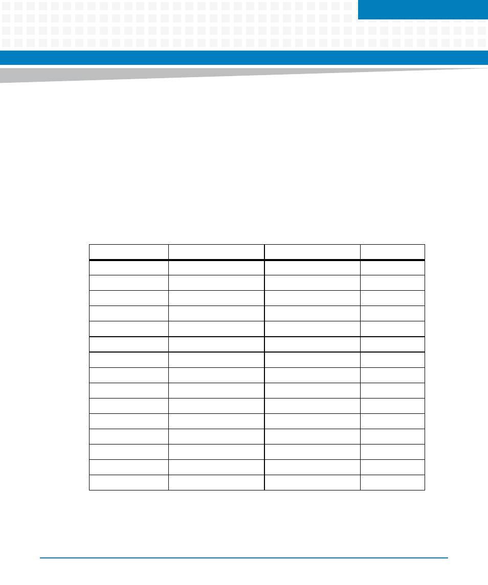
Table 5-1 Physical Address Map
Device Name
Start Address
End Address
Size
DDR
0x0000_0000
0x7fff_ffff
2 GB
PCIE 3 Mem
0x8000_0000
0x9fff_ffff
512 MB
PCIE 2 Mem
0xa000_0000
0xbfff_ffff
512 MB
PCIE 1 Mem
0xc000_0000
0xdfff_ffff
512 MB
PCIE 3 IO
0xffc0_0000
0xffc0_ffff
64 KB
PCIE 2 IO
0xffc1_0000
0xffc1_ffff
64 KB
PCIE 1 IO
0xffc2_0000
0xffc2_ffff
64 KB
UART0
0xffc4_0000
0xffc4_ffff
64 KB
UART1
0xffc5_0000 0xffc5_ffff 64
KB
UART2
0xffc6_0000
0xffc6_ffff
64 KB
UART3
0xffc7_0000
0xffc7_ffff
64 KB
Timer
0xffc8_0000
0xffc8_ffff
64 KB
FPGA
0xffdf_0000 0xffdf_0fff
4
KB
CCSR
0xffe0_0000
0xffef_ffff 1
MB
MRAM
0xfff0_0000
0xfff7_ffff
512 KB