4 lbc timing parameters, Table 7-5, Lbc timing parameters – Artesyn MVME2500 ECC Installation and Use (August 2014) User Manual
Page 126: Programming model
Programming Model
MVME2500-ECC Installation and Use (6806800N30F)
126
7.6.4
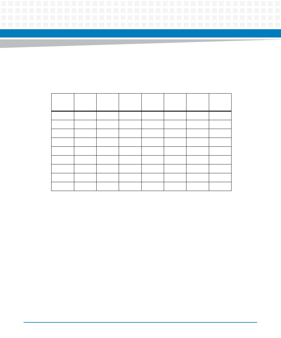
LBC Timing Parameters
The following table defines the timing parameters for the devices on the local bus.
Table 7-5 LBC Timing Parameters
0
1
2
3
4
5
6
MRAM
UART 0
UART 1
UART 2
UART 3
FPGA
Timers
BCTLD
0
0
0
0
0
0
0
CSNT
1
1
1
1
1
1
1
ACS
10
10
10
10
10
10
10
XACS
0
0
0
0
0
0
0
SCY
0011
0011
0011
0011
0011
0011
0011
SETA
0
0
0
0
0
0
0
TRLX
0
0
0
0
0
0
0
EHTR
0
0
0
0
0
0
0
EAD
0
0
0
0
0
0
0
Field Description
BCTLD
Buffer control disable.
0 - LBCTL is asserted upon access to the current memory bank.
CSNT
Chip Select negation time.
1 - LCSn and LWE are negated one quarter of the bus clock cycle earlier
ACS
Address to chip-select setup.
10 - LCSn is outputted one quarter bus clock cycle after the address lines.
XACS
Extra Address to chip-select setup
0 - Address to chip-select setup is determined by ORx[ACS]
SCY
Cycle length in bus clocks
0011 - Three bus clock cycle wait state