Figure 8-2. crc code example – Maxim Integrated Secure Microcontroller User Manual
Page 73
Secure Microcontroller User’s Guide
73 of 187
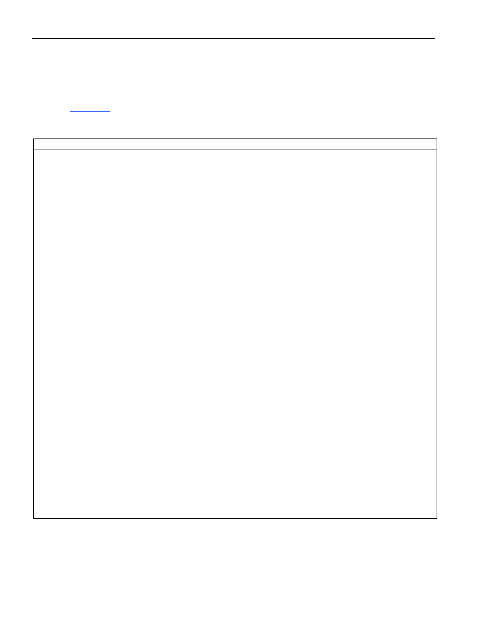
The CRC-16 logic is accessed via the CRCMSB and CRCLSB SFRs mentioned above. The software
must sequentially write the memory values into the CRC LSB at location 0C2h. After a delay of one
instruction cycle, the 16-bit result will be available at 0C3h and 0C2h. When using the CRC-16 hardware
as part of an application, the CRC should first be cleared by writing the LSB back twice with a delay in
between for computation. This process makes the CRC-16 result equal to 0000h. The code example
shown in
displays the CRC-16 result on ports 0 and 1.
Figure 8-2. CRC Code Example
This routine tests the CRC-16 circuit in the DS5001/DS5002FP
crcmsb
equ
0C3h
crclsb
equ
0C2h
org
00h
; after reset, CRC regs = 0000
begin:
mov
p2, crcmsb
;p2 = 00 read crcmsb register
mov
p3, crclsb
;p3 = 00 read crclsb register
mov
crclsb, #075h
;check crc register operation
;data in = 75 result = E7C1
mov
crclsb, #08Ah
;data in = 8A result = 37A7
mov
crclsb, #00Bh
;data in = 0B result = 7D37
mov
crclsb, #075h
;data in = 75 result = 31FD
mov
crclsb, #0C7h
;data in = C7 result = 13B1
mov
crclsb, #0AAh
;data in = AA result = 0B53
mov
crclsb, #075h
;data in = 75 result = DA8A
mov
crclsb, #0C7h
;data in = C7 result = 351A
mov
crclsb, #055h
;data in = 55 result = F474
mov
crclsb, #043h
;data in = 43 result = D6B5
nop
;delay after last write and before first read
;let CRC finish
mov
p0, crcmsb
;p0 = D6 read CRCMSB register
mov
p1, crclsb
;p1 = B5 read CRCLSB register
mov
crclsb ,crclsb
;clear CRC, data in = B5 result = 00D6
nop
;need delay
mov
crclsb ,crclsb
;cleared, data in = D6 result = 0000
nop
mov
p2, crcmsb
;p1 = 00 read crcmsb register
mov
p3, crclsb
;p1 = 00 read crclsb register
end_loop:
sjmp
$
end