3 synchronous operation (mode 0), Ynchronous, Peration – Maxim Integrated Secure Microcontroller User Manual
Page 119: Table 14-b. timer 1 baud rate generation
Secure Microcontroller User’s Guide
119 of 187
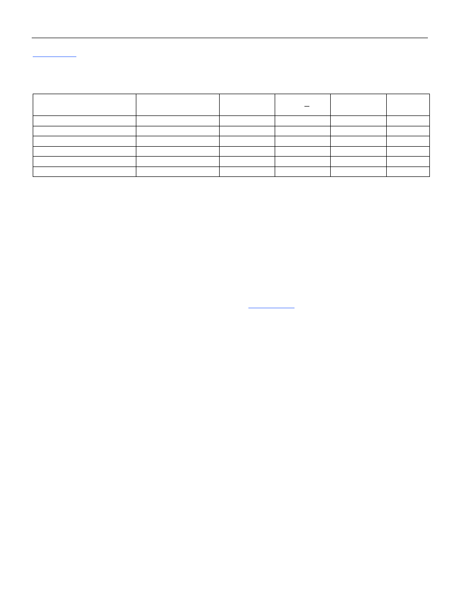
lists some commonly used baud rates that can be derived by using Timer 1 in the timer
configuration described above with an 11.059MHz crystal as the time base.
Table 14-B. Timer 1 Baud Rate Generation
BAUD RATE (BPS)
1/t
CLK
(MHz)
SMOD
(PCON.7)
TIMER 1
C/
T
TIMER
MODE
TH1
19,200
11.059
1
0
2
0FDH
9600
11.059
0
0
2
0FDH
4800
11.059
0
0
2
0FAH
2400
11.059
0
0
2
0F4H
1200
11.059
0
0
2
0E8H
300
11.059
0
0
2
0A0H
When Timer 1 is used in this manner its interrupt should be disabled since the timeout period is much
faster than is reasonable for interrupt response and service by the application software. See the application
note at the end of this section.
14.3 Synchronous Operation (Mode 0)
Mode 0 is the synchronous operating Mode 0 of the serial I/O port. It is intended primarily for
transferring data to external shift registers or for communication with serial peripheral devices. The word
length is eight bits on both transmit and receive. Serial data is both input and output on the RXD pin.
Both transmit and receive data are synchronized to a clock signal which is output on the TXD pin at the
serial data rate fixed at 1/12 of the frequency of the clock oscillator. A block diagram of the serial I/O
port and timing waveforms for Mode 0 is shown in
as a reference for the following
discussion.
Serial data output is initiated following any instruction that causes data to be written to the Transmit Shift
register located at the SBUF register address. At the time that data is written to the Transmit Shift
register, a 1 is simultaneously written to the 9th bit position of the register (D8). The internal WRSBUF
signal is pulsed during S6P2 and data is shifted out LSB first beginning at S6P2 of the next machine
cycle. The contents of the Transmit Shift register are shifted to the right one position during S6P2 of
every machine cycle until D7 has been output. As each shift right operation is performed, a 0 is shifted
into the MSB position from the left. At the end of the D7 bit time, another shift is performed at S6P2 that
loads the output latch of RXD with the 1 that was originally written into bit position D8. During the final
shift register operation, another 0 is shifted in from the left so that the Transmit Shift register contains all
0s. Also at this time, the Transmit Interrupt flag (TI) is set and a serial interrupt will be generated if
enabled.
During serial data transmission in Mode 0, SHCLK is initially driven low onto the TXD pin at S3 of the
machine cycle when D0 is output. During the time that the data word is shifted out, SHCLK will be low
during S3, S4, and S5 and high during S6, S1, and S2 of every machine cycle.
A serial data word will be shifted into the Receive Shift register as soon as the condition REN=1 and
RI=0 is satisfied. This condition can only be initiated by a write to the SCON register from the
application software. At S6P2 of the second machine cycle following the write to SCON, the RXD pin
will be sampled and the value (D0) will be shifted into the MSB position of the Receive Shift register.
Seven more shifts will occur at S6P2 of subsequent machine cycles until the entire 8-bit word has been
shifted into the Receive Shift register.