Figure 5-5 – Maxim Integrated Secure Microcontroller User Manual
Page 55
Secure Microcontroller User’s Guide
55 of 187
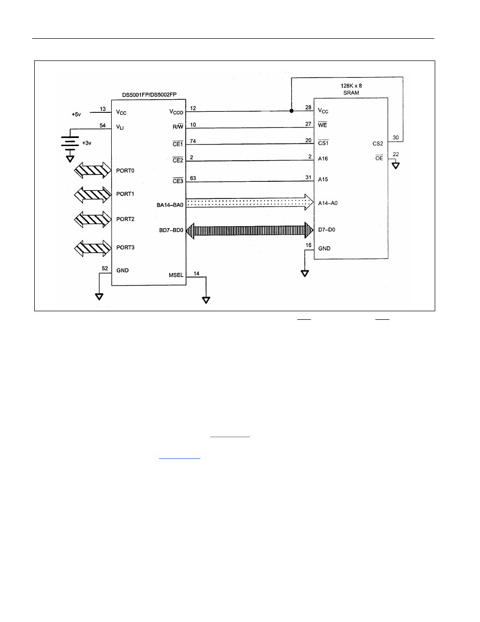
Figure 5-5. Memory Interconnect Using the 128kB SRAM
In the 128kB x 8 configuration, the microprocessor converts the
CE3
into A15 and
CE2
into A16.
Grounding the MSEL pin causes this configuration. The physical location of program memory is between
addresses 0000h to FFFFh. Data memory is located between 10000h and 1FFFFh. These physical
locations are transparent to the user. From a software perspective, both program and data are located
between 0000 and FFFFh. When the MSEL pin is grounded, the device cannot be partitioned. The MSL
bit accessed through the bootstrap loader is used to select access to the 64kB data or 64kB program
segment via the loader in the 128kB x 8 configuration.
The DS2251T 128kB micro stik uses a DS5001FP. The DS2252T secure micro stik is based on the
DS5002FP. The DS5002FP device provides additional memory security features. The modules are
available in 32kB, 64kB, and 128kB versions.
is a block diagram of the DS2251T with 128kB
of NV RAM. This part can also be built with 32kB or 64kB. In this case, the 128kB RAM is replaced
with one or two 32kB RAMs.
shows a DS2252T with 32kB of RAM. This part is also
available in 64kB or 128kB versions. The 64kB version uses two RAMs. The 128kB version uses the
single 128kB SRAM. This is entirely transparent to the user and is provided for completeness.