2 instruction timing, Nstruction, Iming – Maxim Integrated Secure Microcontroller User Manual
Page 131: Figure 15-2. clock source input, Figure 15-2
Secure Microcontroller User’s Guide
131 of 187
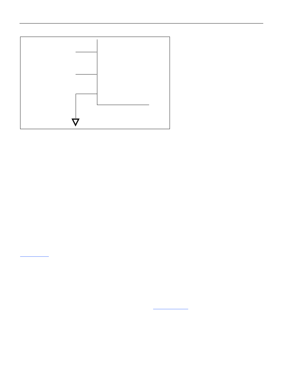
Figure 15-2. Clock Source Input
15.2 Instruction Timing
The internal clocking signals are divided to produce the necessary clock phases, state times, and machine
cycles that define the sequential execution of instructions. Two clock oscillator periods define one state
time. The first clock-oscillator pulse period of a state time is called the Phase 1 clock. Tthe second is
called the Phase 2 clock. In general, arithmetic and logical operations take place during Phase 1 and
internal register-to-register transfers take place during Phase 2.
A machine-cycle is composed of 12 oscillator periods or six state times. The state times within the
machine cycle are numbered S1 through S6. Each clock oscillator period within the machine cycle is
designated according to the state number and the phase it represents within the state. Thus, the oscillator
periods are numbered S1P1 (State 1, Phase 1) through S6P2 (State 6, Phase 2).
All the instruction sequences executed by the CPU are preceded by a single byte (8-bit) op code and
consist of one, two, or three bytes. Most of the instructions execute in one machine cycle. The rest of the
instructions execute in two machine cycles, except for multiply (MUL) and divide (DIV), which execute
in four cycles each.
is a timing diagram illustrating the memory access and execution timing for typical
instructions when they are executed from bytewide RAM. The timing shown is referenced to the
internally generated machine cycles composed of state times and clock oscillator phases. The relationship
between the internal instruction execution timing and the external signals XTAL2 and ALE is illustrated
in the diagram. Except for the MOVX instructions, two code bytes from program nemory are always read
during each machine cycle of instruction execution. These read operations take place at state times S1 and
S4.
Execution of a 1-byte, 1-cycle instruction is illustrated in
. It begins with the op-code byte
fetch that occurs during S1 and the op-code byte is latched into the instruction register at S1P2. The code
byte, which is read during S4, in this case, is actually the op-code byte of the next instruction. This byte is
effectively discarded and the program counter is not incremented. Execution of the instruction is
completed S6P2, the end of the machine cycle.
GND
XTAL1
XTAL2
N.C.
EXTERNAL
OSCILLATOR
SIGNAL