6 design notes, Esign, Otes – IEI Integration ICE-DB-T6 User Manual
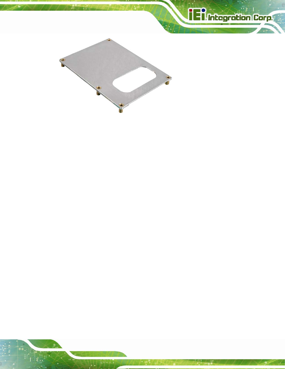
Page 91: Figure 5-9: iei heat spread module
Type 6 Carrier Board Design Guide
Page 81
Figure 5-9: IEI Heat Spread Module
5.6 Design Notes
5.6.1 Component Height — Module Back and Carrier Board Top
Parts mounted on the backside of the module (in the space between the bottom surface of
the module PCB and the carrier board) shall have a maximum height of 3.8 mm
(dimension ‘B’ in Figure 5-10). With the 5 mm stack option, the clearance between the
carrier board and the bottom surface of the module’s PCB is 5 mm (dimension ‘A’ in Figure
5-10). Using the 5 mm stack option, components placed on the carrier board topside
under the module envelope shall be limited to a maximum height of 1 mm (dimension ‘C’
in Figure 5-10), with the exception of the mating connectors. Using carrier board topside
components up to 1mm allows a gap of 0.2 mm between carrier board module bottom side
components. This may not be sufficient in some situations. In carrier board applications in
which vibration or board flex is a concern, then the carrier board component height should
be restricted to a value less than 1mm that yields a clearance that is sufficient for the
application. If the carrier board uses the 8 mm stack option (dimension ‘A’ in Figure 5-10),
then the carrier board topside components within the module envelope shall be limited to
a height of 4 mm (dimension ‘C’ in Figure 5-10), with the exception of the mating
connectors. Using carrier board topside components up to 4mm allows a gap of 0.2 mm
between carrier board topside components and module bottom side components. This
may not be sufficient in some situations. In carrier board applications in which vibration or
board flex is a concern, then the carrier board component height should be restricted to a
value less than 4 mm that yields a clearance that is sufficient for the application.