5 pci express routing guideline, 1 impedance consideration, Table 3-2: pci express impedance consideration – IEI Integration ICE-DB-T6 User Manual
Page 34
Type 6 Carrier Board Design Guide
Page 24
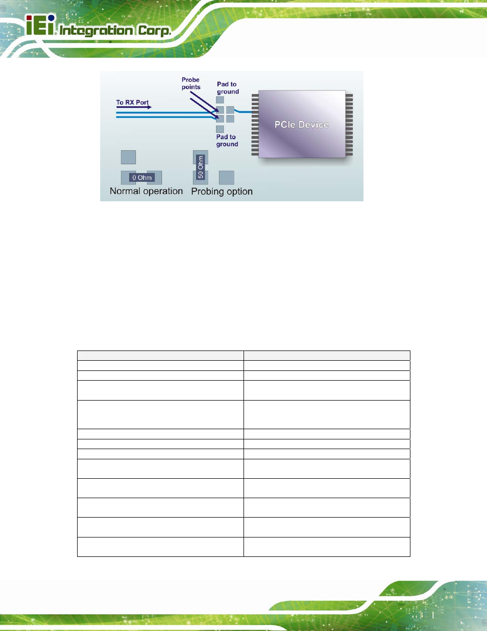
Figure 3-2: Intel Recommend Test Structure for PCI Express Data Eye Measurement
3.1.5 PCI Express Routing Guideline
3.1.5.1 Impedance Consideration
The PCI Express impedance considerations are listed in Table 3-2.
Table 3-2: PCI Express Impedance Consideration
Parameters
Routing
Transfer Rate / PCIe Lane
2.5 Gbits/sec
Maximum signal line length (coupled traces) TX and RX path: 21.0 inches
Maximum signal length allowance on the
COM Express module "
TX and RX path: 5.15 inches
Signal length allowance on the COM
Express carrier board "
TX and RX path: 15.85 inches @
0.28dB/GHz/inch to PCIe device 9.00 inches
@ 0.28dB/GHz/inch to PCIe slot
Differential Impedance
100 Ohms +/-20%
Single-ended Impedance
55 Ohms +/-15%
Trace width (W)
5 mils (microstrip routing) (*)
Spacing between differential pairs (intra-pair)
(S)
4 mils (microstrip routing) (*)
Spacing between RX and TX pairs
(inter-pair) (s)
Min. 20mils
Spacing between differential pairs and
high-speed periodic signals
Min. 50mils
Spacing between differential pairs and
low-speed non periodic signals
Min. 20mils
Length matching between differential pairs
(intra-pair)
Max. 5mils