6 usb routing guideline, 1 impedance, 2 general routing and placement – IEI Integration ICE-DB-T6 User Manual
Page 52

Type 6 Carrier Board Design Guide
Page 42
3.4.6 USB Routing Guideline
3.4.6.1 Impedance
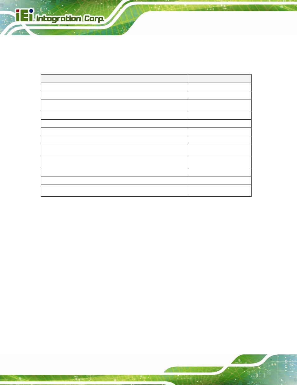
Parameters
Routing
Transfer rate / Port
480 Mbit/s
Maximum signal line length (coupled traces)
Max. 17.0 inches
Signal length used on COM Express module (including the COM
Express" connector) "
3.0 inches
Signal length allowance for the COM Express carrier board "
14.0 inches
Differential Impedance
90 Ohms +/-15%
Single-ended Impedance
45 Ohms +/-10%
Spacing between pairs-to-pairs (inter-pair) (s)
Min. 20mils
Spacing between differential pairs and high-speed periodic
signals
Min. 50mils
Spacing between differential pairs and low-speed non periodic
signals
Min. 20mils
Reference plain
GND referenced preferred
Spacing from edge of plane
Min. 40mils
Via Usage
Try to minimize number of
vias
3.4.6.2 General Routing and Placement
USB 2.0 signals should be ground referenced.
Route USB 2.0 signals using a minimum of vias and corners. This reduces
reflections and impedance changes.
When it becomes necessary to turn 90°, use two 45° turns or an arc instead of
making a single 90° turn. This reduces reflections on the signal by minimizing
impedance discontinuities.
Do not route USB 2.0 traces under crystals, oscillators, clock synthesizers,
magnetic devices or ICs that use and/or duplicate clocks.
Avoid stubs on high-speed USB signals, as stubs will cause signal reflections and
affect signal quality. If a stub is unavoidable in the design, the total of all the stubs
on a particular line should not be greater than 200 mils.
Route all traces over continuous planes, with no interruptions. Avoid crossing over
anti-etch if possible. Crossing over anti-etch (plane splits) increases inductance
and radiation levels by forcing a greater loop area. Likewise, avoid changing
