2 lvds cable consideration, 3 backlight and lcd power timing control, Table 3-14: lvds signals description – IEI Integration ICE-DB-T6 User Manual
Page 58
Type 6 Carrier Board Design Guide
Page 48
CMOS
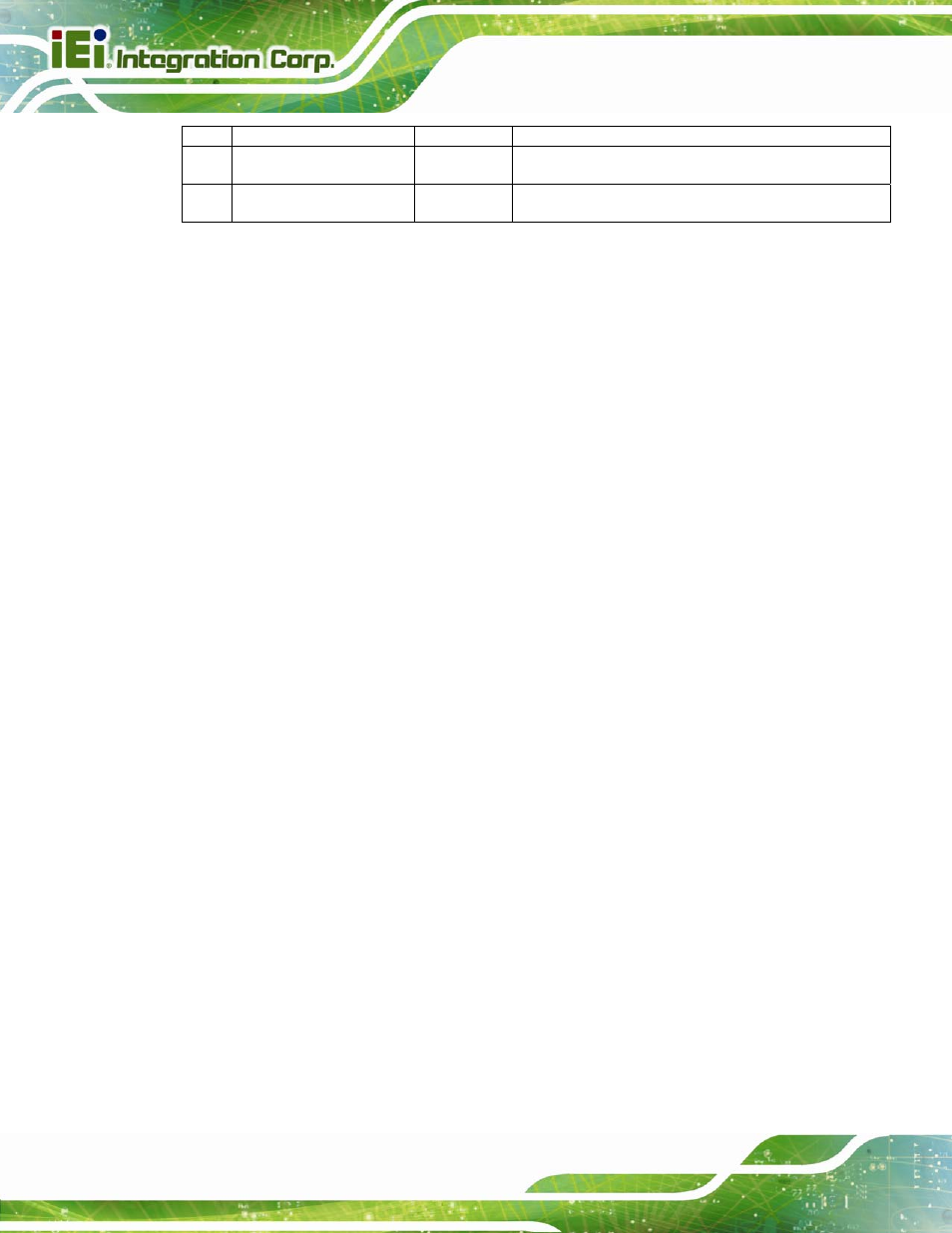
A83 LVDS_I2C_CK
O 3.3V
CMOS
DDC I2C clock signal used for flat panel detection
and control.
A84 LVDS_I2C_DAT
I/O 3.3V
OD CMOS
DDC I2C data signal used for flat panel detection
and control.
Table 3-14: LVDS Signals Description
3.6.2 LVDS Cable Consideration
Balanced cables (twisted pair) are usually better than unbalanced cables (ribbon cable)
for noise reduction and signal quality. Balanced cables provide a low-cost solution with
good balance and flexibility. They tend to generate less EMI due to field canceling effects
and also tend to pick up electromagnetic radiation as common-mode noise, which is
rejected by the receiver. They are capable of medium to long runs.
Unbalanced cables are a cost effective and easy solution. They work fine for very short
runs even though they are not well suited for high-speed differential signaling. Most cables
will work effectively for cable distances of <0.5m.
3.6.3 Backlight and LCD Power Timing Control
Figure 3-19 and Figure 3-20 show the reference design of backlight and LCD power timing
control. Figure 3-21 shows the LCD power sequence, and design must conform to its
power sequence. VIN represents LCD power and lamp represents LCD backlight power.