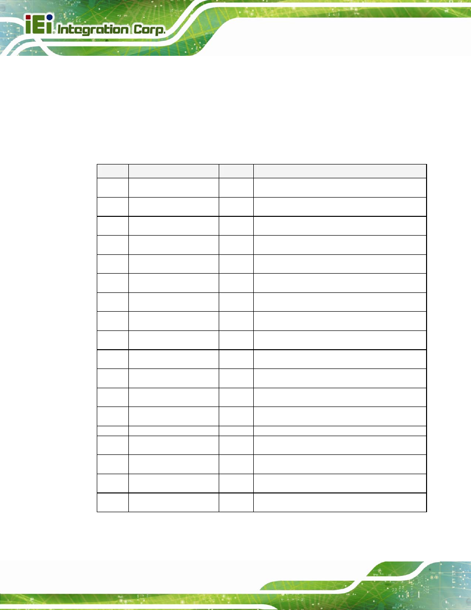
1 signal description, Table 3-3: pci express signal descriptions – IEI Integration ICE-DB-T6 User Manual
Page 38
Type 6 Carrier Board Design Guide
Page 28
The PCI Express interface of the COM Express module consists of up to six lanes, each
with a receive and transmit differential signal pair. According to the PCI Express
specification, these six lanes can be configured as several PCI Express x1 links or to a
combined x4 link plus two x1 links. These configuration possibilities are based on the
COM Express module's chipset capabilities.
3.2.1 Signal Description
Pin
Signal
I/O
Description
B68
B69
PCIE_RX0+
PCIE_RX0-
I
PCIe Port 0. Receive Input differential pair.
A68
A69
PCIE_TX0+
PCIE_TX0-
O
PCIe Port 0. Transmit Output differential pair.
B64
B65
PCIE_RX1+
PCIE_RX1-
I
PCIe Port 1. Receive Input differential pair.
A64
A65
PCIE_TX1+
PCIE_TX1-
O
PCIe Port 1. Transmit Output differential pair.
B61
B62
PCIE_RX2+
PCIE_RX2-
I
PCIe Port 2. Receive Input differential pair.
A61
A62
PCIE_TX2+
PCIE_TX2-
O
PCIe Port 2. Transmit Output differential pair.
B58
B59
PCIE_RX3+
PCIE_RX3-
I
PCIe Port 3. Receive Input differential pair.
A58
A59
PCIE_TX3+
PCIE_TX3-
O
PCIe Port 3. Transmit Output differential pair.
B55
B56
PCIE_RX4+
PCIE_RX4-
I
PCIe Port 4. Receive Input differential pair.
A55
A56
PCIE_TX4+
PCIE_TX4-
O
PCIe Port 4. Transmit Output differential pair.
B52
B53
PCIE_RX5+
PCIE_RX5-
I
PCIe Port 5. Receive Input differential pair.
A52
A53
PCIE_TX5+
PCIE_TX5-
O
PCIe Port 5. Transmit Output differential pair.
A88
A89
PCIE_CLK_REF+
PCIE_CLK_REF-
O
PCIe Reference Clock for all COM Express
PCIe lanes, and for PEG lanes
B66
WAKE0#
I PCIE
PCIe Wake Event: Sideband wake-up signal.
A49 EXCD0_CPPE#
I
3.3V
CMOS
ExpressCard capable card request, slot 1.
B48 EXCD1_CPPE#
I
3.3V
CMOS
ExpressCard capable card request, slot 2.
A48 EXCD0_PERST#
O
3.3V
CMOS
ExpressCard reset, slot 1.
B47 EXCD1_PERST#
O
3.3V
CMOS
ExpressCard reset, slot 2.
Table 3-3: PCI Express Signal Descriptions