12 miscellaneous, 1 signal description, Iscellaneous – IEI Integration ICE-DB-T6 User Manual
Page 72: Figure 3-28: vga reference design, Type 6 carrier board design guide page 62
Type 6 Carrier Board Design Guide
Page 62
R161
0_4
1
2
R160
33_4
1
2
VGA_HSYNC
VGA_VSYNC
VGA_BLU
VGA_GRN
VGA_RED
+V5
+V3.3
VGA_I2C_CK
R156
@2.2K_4
1
2
R158
@2.7K_4
1
2
Q6
@2N7002_SOT23
D
G
S
+V3.3
VGA_I2C_DAT_Z
C127
@22P_4_N_50V
CRT_R
CRT_B
C126
@22P_4_N_50V
IO_GND
VGA_I2C_CK_Z
IO_GND
VGA_I2C_CK_Z
R162
33_4
1
2
IO_GND
R164
33_4
1
2
IO_GND
R165
33_4
1
2
IO_GND
VGA
IO_GND
CRT_R_Y
IO_GND
CON7
VGA SOCKET
<1ST PART FIELD>
1
2
3
4
5
6
7
8
9
10
11
12
13
14
15
16
17
C124
22P_4_N_50V
C121
22P_4_N_50V
R166
0_4
1
2
R155
150_4_1%
+V3.3
R157
@2.7K_4
1
2
R159
@2.2K_4
1
2
+V5
VGA_I2C_DAT
CRT_R_Y
CRT_B_Y
R163
150_4_1%
CRT_G_Y
R167
150_4_1%
L4
FB47_6_300MA
C123
10P_4_N_50V
C125
10P_4_N_50V
C122
10P_4_N_50V
C120
10P_4_N_50V
C117
10P_4_N_50V
C119
10P_4_N_50V
C118
22P_4_N_50V
L5
FB47_6_300MA
L6
FB47_6_300MA
L8
FB47_6_300MA
L7
FB47_6_300MA
IO_GND
L3
FB47_6_300MA
D3
BAV99LT1G_SOT23
A
C
K
+V3.3
CRT_VSYNC
CRT_HSYNC
+V3.3
D5
BAV99LT1G_SOT23
A
C
K
+V3.3
D4
BAV99LT1G_SOT23
A
C
K
CRT_VSYNC
CRT_HSYNC
VGA_I2C_DAT_Z
IO_GND
+V3.3
D1
BAV99LT1G_SOT23
A
C
K
Q7
@2N7002_SOT23
D
G
S
CRT_DDCDATA
+V3.3
+V3.3
D2
BAV99LT1G_SOT23
A
C
K
CRT_DDCCLK
VGA_I2C_DAT
CRT_G
VGA_I2C_CK
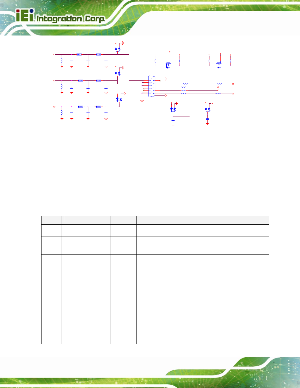
Figure 3-28: VGA Reference Design
3.12 Miscellaneous
This section describes some signals which are not described above, including PI[3:0],
GPO[3:0], Watch Dog Timer, Speaker Out, System Reset, Carrier Board Reset, Suspend
Control, Power Good, Smart Fan Control, I2C Data, Alert#.
3.12.1 Signal Description
Pin
Signal
I/O
Description
B12
PWRBTN#
I CMOS
Power button to bring system out of S5 (soft off), active on
rising edge.
B49
SYS_RESET#
I CMOS Reset button input. Active low input. System is held in
hardware reset while this input is low, and comes out of
reset upon release.
B50
CB_RESET#
O CMOS Reset output from module to Carrier Board. Active low.
Issued by module chipset and may result from a low
SYS_RESET# input, a low PWR_OK input, a VCC_12V
power input that falls below the minimum specification, a
watchdog timeout, or may be initiated by the module
software.
B24
PWR_OK
I CMOS
Power OK from main power supply. A high value indicates
that the power
B18 SUS_STAT#
O
CMOS
Indicates
imminent
suspend operation; used to notify LPC
devices.
A15
SUS_S3#
O CMOS
Indicates system is in Suspend to RAM state. Active low
output.
A18
SUS_S4#
O CMOS
Indicates system is in Suspend to Disk state. Active low
output.
A24 SUS_S5#
O CMOS
Indicates system is in Soft Off state. Also known as