3 routing notices, Figure 3-3: peg lane connection topology example – IEI Integration ICE-DB-T6 User Manual
Page 36
Type 6 Carrier Board Design Guide
Page 26
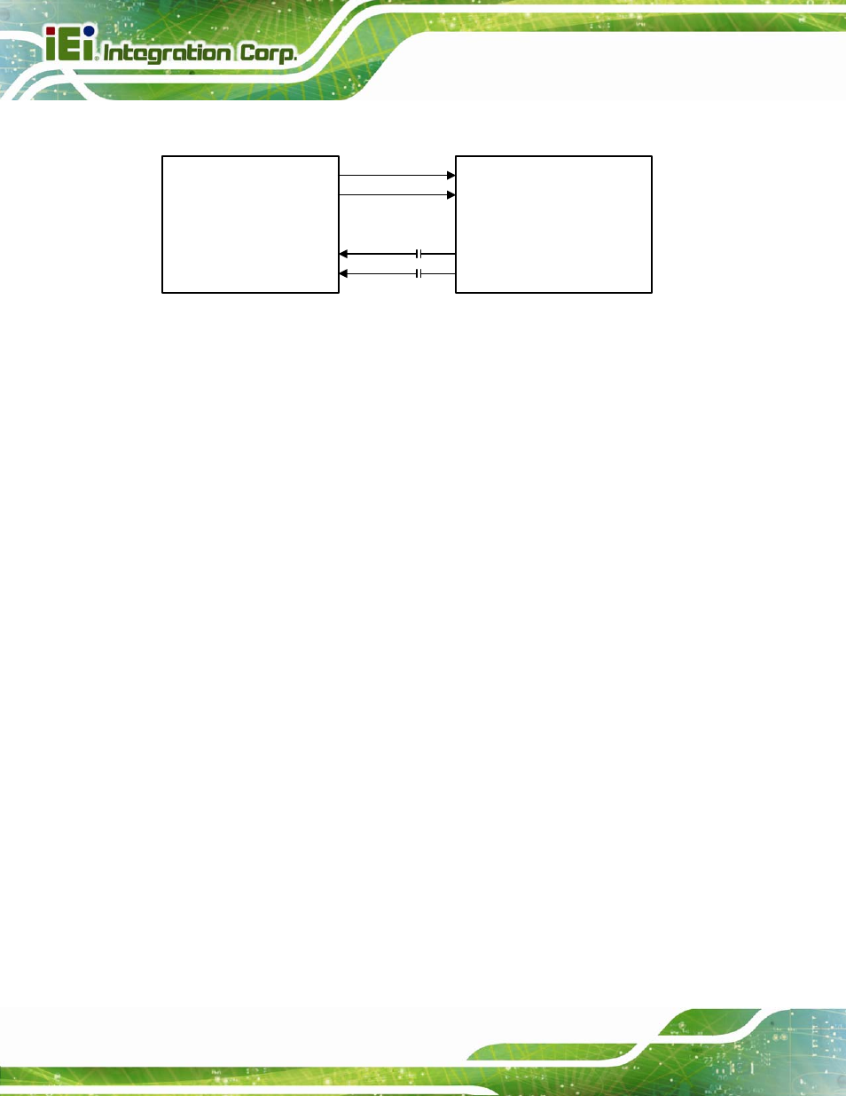
ICE Module
PEG SLOT or SDVO Device
TX+
TX-
RX+
RX-
AC Coupling Cap
Figure 3-3: PEG Lane Connection Topology Example
3.1.5.3 Routing Notices
Each signal and its complement in a differential pair should be length
matched whenever possible on a segment-by-segment basis at the point of
discontinuity. Examples of segments might include breakout areas, routes to
connect vias, routes to connect an AC coupling capacitor, routes to connect a
connector, and so forth.
When trace length matching occurs, it should be made as close as possible to
the point where the length variation occurs, as shown in Figure 3-4. For
example, length matching in a chipset breakout area or connector pin field
should occur within the first 125 mils (3.175 mm) of the structure that causes
the length mismatch.
When serpentining is needed to match lengths, the trace spacing should not
become greater than two times the original spacing. The length of the
increased spacing should not be greater than three times the trace width. See
Figure 3-4. In determining the overall length of a given signal in a differential
pair, use pad or pin edge-to-edge distances rather than the total etch present,
unless the amount of trace routing inside each pad is identical. The amount of
etch within a given pad is electrically part of the pad itself. In other words, only
the etch outside of the pad edge is relevant to the overall length of a
differential pair.