3 sata (serial ata interface), 1 signal description, Sata – IEI Integration ICE-DB-T6 User Manual
Page 43: Erial, Nterface, Figure 3-10: pci express clock buffer example, Type 6 carrier board design guide page 33
Type 6 Carrier Board Design Guide
Page 33
CLK100M_PCIEx1_SLOT2+
5
R20
33_4
1
2
CLK100M_PCIEx1_SLOT2-
5
R21
33_4
1
2
CLK100M_PCIEx16_SLOT- 6
CLK100M_PCIEx16_SLOT+ 6
R24
33_4
1
2
CLK_OE_4
R26
33_4
1
2
CLK_OE_3
SMB_DAT
3,5,6,10,11,17,20
SMB_CK
3,5,6,10,11,17,20
CLK_PLL
CLK100M_PCIEx1_SLOT5- 10
CLK100M_PCIEx1_SLOT5+ 10
CLK100M_PCIEx1_SLOT3-
5
CLK100M_PCIEx1_SLOT3+
5
R22
33_4
1
2
R23
33_4
1
2
R113
33_4
1
2
R112
33_4
1
2
+V3.3_CLK
+V3.3_CLK
+V3.3_CLK_A
CLK_OE_6
CLK100M_PCIEx1_SLOT1+
5
CLK_LOCK
CLK_OE_1
R10
475
R114
33_4
1
2
CLK_IREF
R115
33_4
1
2
CLK100M_PCIEx1_SLOT1-
5
CLK100M_PCIEx1_SLOT4+
5
R25
33_4
1
2
CLK100M_PCIEx1_SLOT4-
5
R27
33_4
1
2
CLK100M_PCIE_REF-
3
CLK100M_PCIE_REF+
3
R16
33_4
1
2
CLK_OE_5
R18
33_4
1
2
CLK_OE_2
CLK100M_PCIEx1_SLOT6- 10
CLK100M_PCIEx1_SLOT6+ 10
CLK_HBW#
CLK_SRC_SOP#
CLK_PD#
U1
ICS9DB801
SRC_DIV#
1
VDD01
2
GND01
3
SRC_IN
4
SRC_IN#
5
OE_0
6
OE_3
7
DIF_0
8
DIF_0#
9
GND02
10
VDD02
11
DIF_1
12
DIF_1#
13
OE_1
14
OE_2
15
DIF_2
16
DIF_2#
17
GND03
18
VDD03
19
DIF_3
20
DIF_3#
21
BYPASS#/PLL
22
SCLK
23
SDATA
24
GND05
25
PD#
26
SRC_SOP#
27
HIGH_BW#
28
DIF_4#
29
DIF_4
30
VDD05
31
GND04
32
DIF_5#
33
DIF_5
34
OE_5
35
OE_6
36
DIF_6#
37
DIF_6
38
VDD04
39
OE_INV
40
DIF_7#
41
DIF_7
42
OE_4
43
OE_7
44
LOCK
45
IREF
46
GNDA
47
VDDA
48
CLK_OE_7
TP32
1
CLK_DIV#
TP33
1
CLK_OE_0
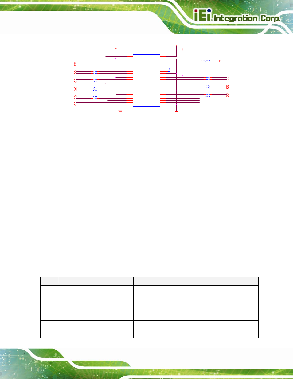
Figure 3-10: PCI Express Clock Buffer Example
3.3 SATA (Serial ATA Interface)
Serial ATA is a serial interface for connecting storage devices (mainly hard disks). SATA
uses a point-to-point serial connection between the system and the storage device. The
first-generation SATA provides a maximum data transfer rate of 1.5Gb/s per port. The
second generation SATA 3Gb/s provides transfer rate of up to 3Gb/s per port while the
third generation SATA 6Gb/s provides transfer rate of up to 6Gb/s. Serial ATA is
completely software transparent to the IDE interface while providing a lower pin count and
higher performance.
3.3.1 Signal Description
All COM Express modules provide up to four Serial ATA channels, each with a receive
and transmit differential signal pair. The appropriate signals can be found on the COM
Express module connector row A and row B.
Pin
Signal
I/O
Description
A19
A20
SATA0_RX+
SATA0_RX-
I SATA
Serial ATA channel 0 Receive input differential pair.
A16
A17
SATA0_TX+
SATA0_TX-
O SATA
Serial ATA channel 0 Transmit output differential pair.
B19
B20
SATA1_RX+
SATA1_RX-
I SATA
Serial ATA channel 1 Receive input differential pair.
B16
B17
SATA1_TX+
SATA1_TX-
O SATA
Serial ATA channel 1 Transmit output differential pair.
A25
SATA2_RX+
I SATA
Serial ATA channel 2 Receive input differential pair.