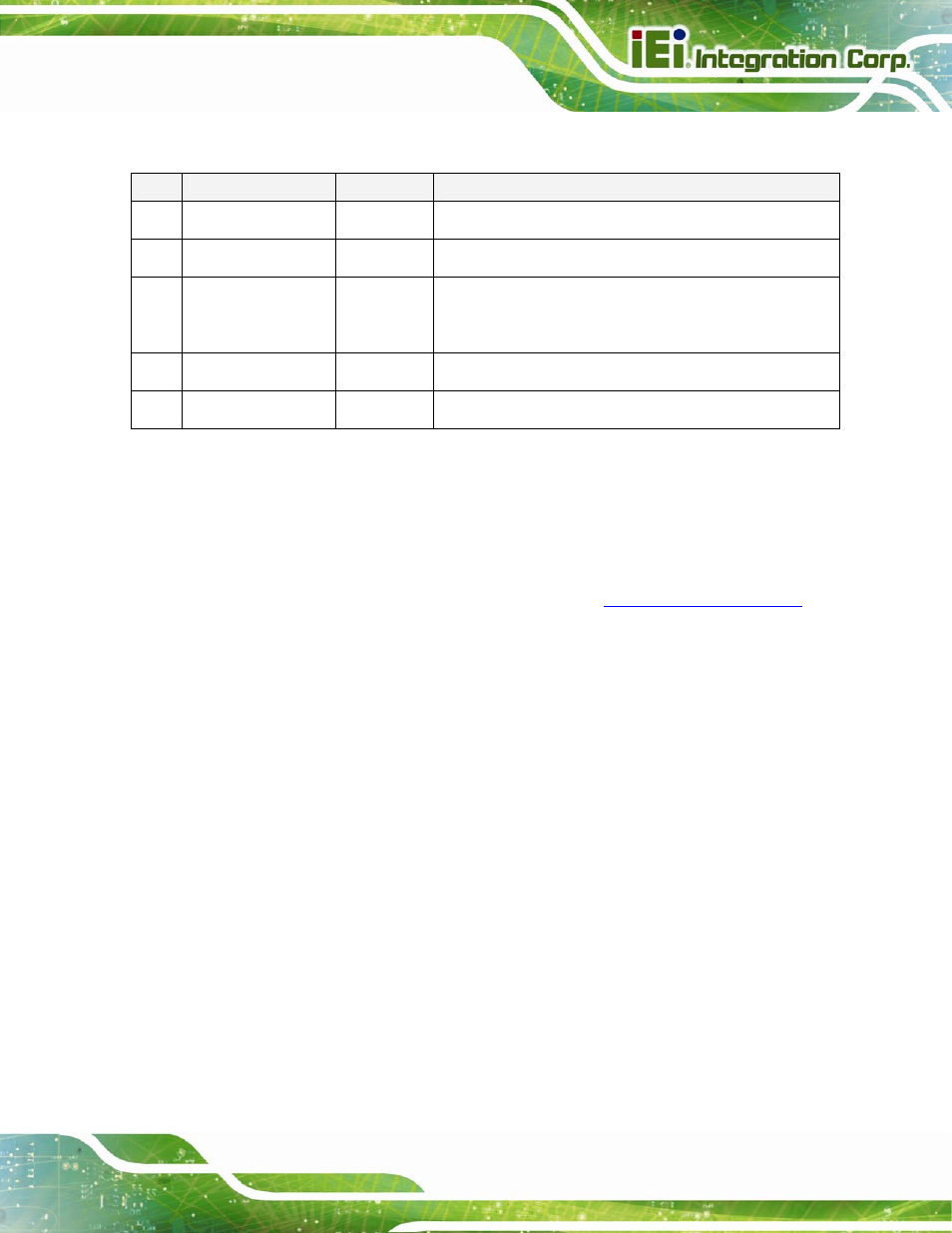
2 lpc super io for legacy io support, Table 3-19: lpc interface signal descriptions – IEI Integration ICE-DB-T6 User Manual
Page 67
Type 6 Carrier Board Design Guide
Page 57
Pin
Signal
I/O
Description
A50 LPC_SERIRQ
I/O 3.3V
CMOS
LPC serialized IRQ.
B3 LPC_FRAME#
O 3.3V
CMOS
LPC frame indicates start of a new cycle or termination
of a broken cycle.
B4
B5
B6
B7
LPC_AD0
LPC_AD1
LPC_AD2
LPC_AD3
I/O 3.3V
CMOS
LPC multiplexed command, address and data.
B8
B9
LPC_DRQ0#
LPC_DRQ1#
I 3.3V
CMOS
LPC encoded DMA/Bus master request.
B10 LPC_CLK
O 3.3V
CMOS
LPC clock output 33MHz.
Table 3-19: LPC Interface Signal Descriptions
3.10.2 LPC Super IO for Legacy IO Support
Some of the IEI COM Express modules utilize BIOS that contains built-in support for an
external Winbond W83627DHG LPC Super I/O controlle
The base address for this Super I/O should be 0x2E to be sure that the legacy devices can
be initialized by the BIOS. The implementation of the COM Express module on the carrier
board will provide legacy interfaces such as PS/2 keyboard/mouse and two serial ports
(COM1 and COM2). The other functions of this Super I/O controller are not supported.