3 esd/emi, Table 3-8: usb connector signal description, Type 6 carrier board design guide page 39 – IEI Integration ICE-DB-T6 User Manual
Page 49
Type 6 Carrier Board Design Guide
Page 39
Pin
Signal
I/O
Description
1
VCC
P
+5V Power supply
2
DATA-
I/O
USB Data, negative differential signal.
3
DATA+
I/O
USB Data, positive differential signal.
4 GND
P
Ground
Table 3-8: USB Connector Signal Description
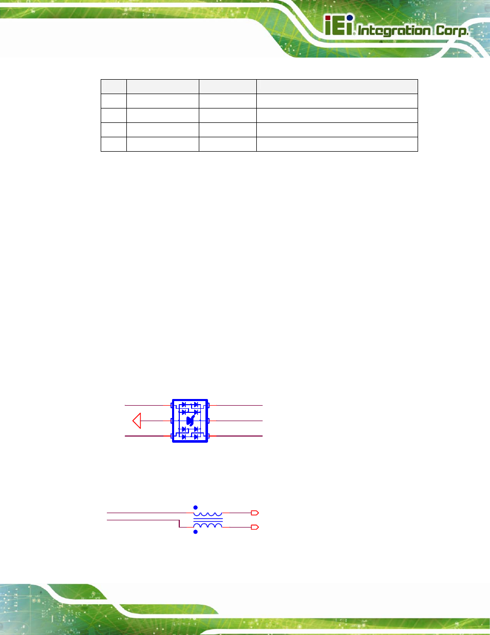
3.4.3 ESD/EMI
To improve the EMI behavior of the USB interface, common mode choke should be
included in a design. Common mode chokes have to be placed as close as possible to the
USB connector signal pins to provide required noise attenuation, but they also distort the
signal quality of full-speed and high-speed signaling. Therefore, common mode chokes
should be chosen carefully to meet the requirements of the EMI noise filtering while
retaining the integrity of the USB signals on the carrier board design.
Low capacitance steering diodes and transient voltage suppression diodes have to be
implemented on the carrier board design to protect the USB host interface of the module
from over-voltage caused by electrostatic discharge (ESD) and electrical fast transients
(EFT).
IO_GND
USB0-_R
USB1-_R
D10
PACDN006
1
2
3
4
5
6
USB1+_R
USB0+_R
+V5_USB01
Figure 3-15: RailClamp SRV05-4
Low Capacitance TVS Diode Array for ESD
USB1-_R
USB1+_R
USB1-
3
USB1+
3
L17
COMCHOKE_8_USB
1
4
2
3
Figure 3-16: 90 ohm Common Mode Choke at 100MHz for EMI