Audio output interface, Description – Rainbow Electronics AT89C5132 User Manual
Page 61
61
AT8xC5132
4173A–8051–08/02
Audio Output
Interface
The AT8xC5132 implement an audio output interface allowing the audio bitstream to be
output in various formats. It is compatible with right and left justification PCM and I
2
S for-
mats and thanks to the on-chip PLL (see Section “Clock Controller”, page 12) allows
connection of almost all of the commercial audio DAC families available on the market.
Description
The C51 core interfaces to the audio interface through five special function registers:
AUDCON0 and AUDCON1, the Audio Control registers (see Table 67 and Table 68);
AUDSTA, the Audio Status register (see Table 69); AUDDAT, the Audio Data register
(see Table 70); and AUDCLK, the Audio Clock Divider register (see Table 71).
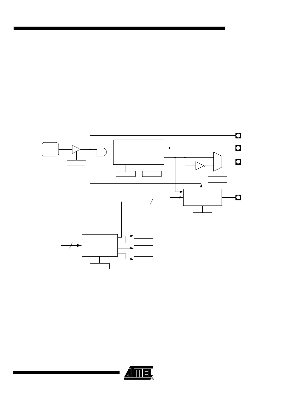
Figure 40 shows the audio interface block diagram, blocks are detailed in the following
sections.
Figure 40. Audio Interface Block Diagram
AUD
CLOCK
UDRN
AUDSTA.6
0
1
DSIZ
AUDCON0.1
DSEL
Clock Generator
DCLK
DOUT
SCLK
JUST4:0
AUDCON0.7:3
POL
AUDCON0.2
AUDEN
AUDCON1.0
HLR
AUDCON0.0
8
Data Converter
Audio Data
From C51
DUP1:0
AUDCON1.2:1
SREQ
AUDSTA.7
Audio Buffer
AUBUSY
AUDSTA.5
Data Ready
AUDDAT
16