Registers, Table 16) – Rainbow Electronics AT89C5132 User Manual
Page 15
15
AT8xC5132
4173A–8051–08/02
Registers
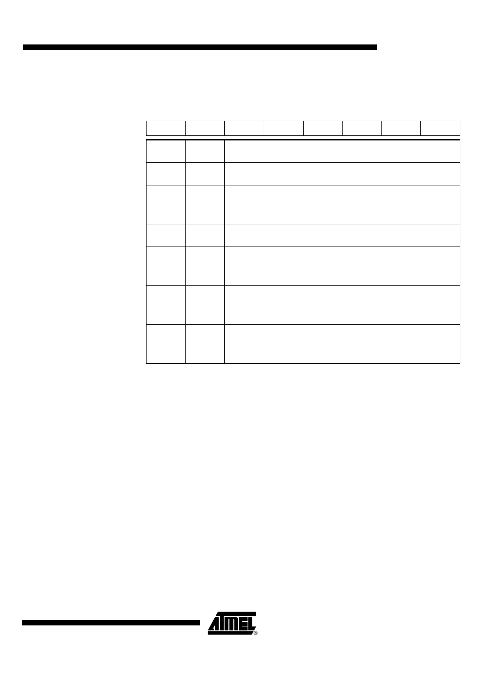
Table 16. CKCON Register
CKCON (S:8Fh) – Clock Control Register
Reset Value = 0000 000Xb
7
6
5
4
3
2
1
0
-
WDX2
-
-
-
T1X2
T0X2
X2
Bit
Number
Bit
Mnemonic
Description
7
-
Reserved
The values read from this bit is indeterminate. Do not set this bit.
6
WDX2
Watchdog Clock Control Bit
Set to select the oscillator clock divided by two as watchdog clock input (X2
independent).
Clear to select the peripheral clock as watchdog clock input (X2 dependent).
5 - 3
-
Reserved
The values read from these Bits are indeterminate. Do not set these Bits.
2
T1X2
Timer 1 Clock Control Bit
Set to select the oscillator clock divided by two as Timer 1 clock input (X2
independent).
Clear to select the peripheral clock as Timer 1 clock input (X2 dependent).
1
T0X2
Timer 0 Clock Control Bit
Set to select the oscillator clock divided by two as timer 0 clock input (X2
independent).
Clear to select the peripheral clock as timer 0 clock input (X2 dependent).
0
X2
System Clock Control Bit
Clear to select 12 clock periods per machine cycle (STD mode, F
CPU
= F
PER
=
F
OSC
/
2).
Set to select 6 clock periods per machine cycle (X2 mode, F
CPU
= F
PER
= F
OSC
).