E figure 73 s – Rainbow Electronics AT89C5132 User Manual
Page 105
105
AT8xC5132
4173A–8051–08/02
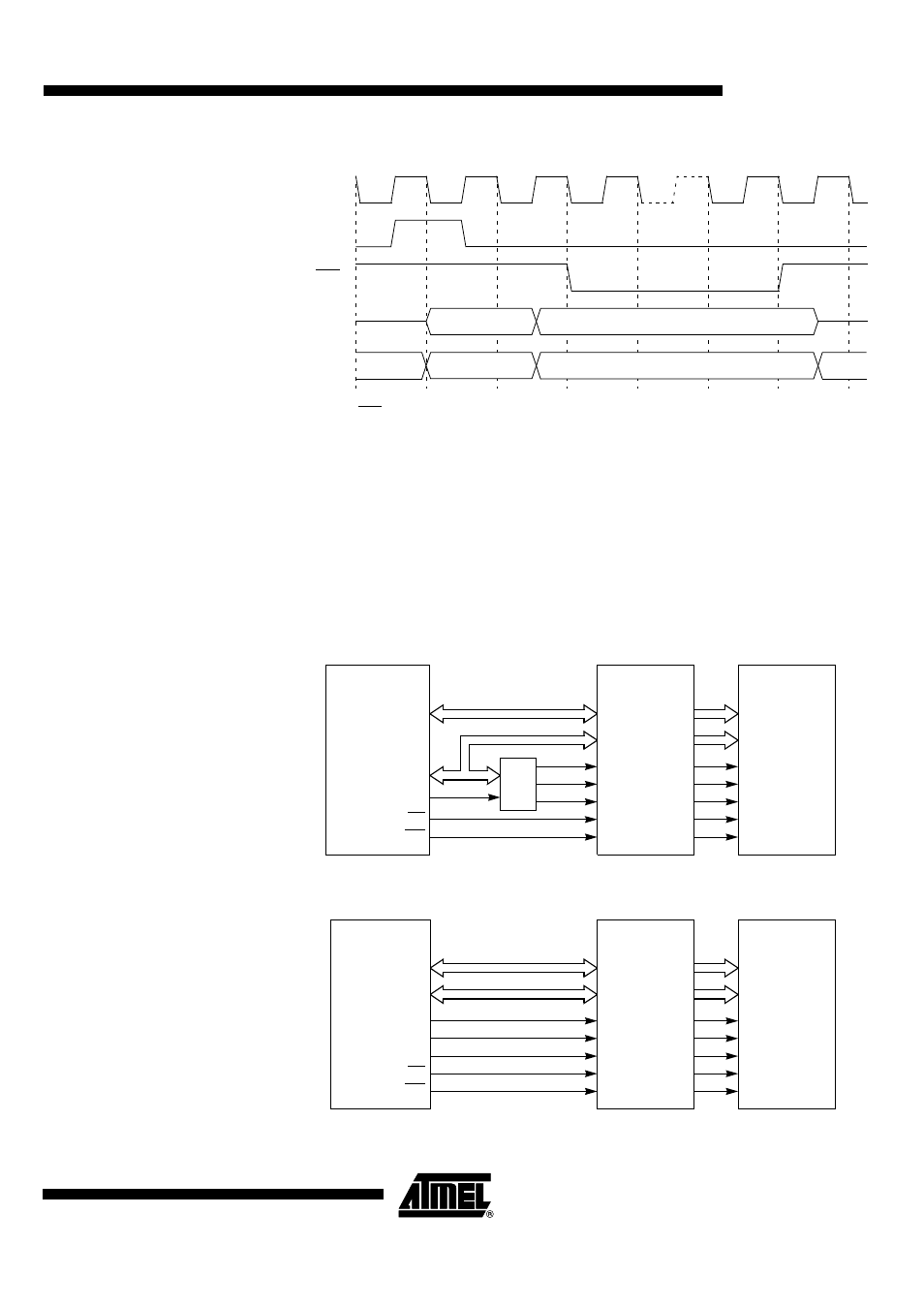
Figure 73. IDE Write Waveforms
Notes:
1. WR signal may be stretched using M0 bit in AUXR register.
2. When executing MOVX @Ri instruction, P2 outputs SFR content.
3. When executing MOVX @DPTR instruction, if DPHDIS is set (Page Access Mode),
P2 outputs SFR content instead of DPH.
IDE Device Connection
Figure 74 and Figure 75 show two examples on how to interface up to two IDE devices
to the AT8xC5132. In both examples P0 carries IDE low order data Bits D7:0, P2 carries
IDE high order data Bits D15:8, while RD# and WR# signals are respectively connected
to the IDE nIOR and nIOW signals. Other IDE control signals are generated by the
address latch outputs in the first example – they are generated by port I/Os in the sec-
ond example.
Figure 74. IDE Device Connection Example 1
Figure 75. IDE Device Connection Example 2
ALE
P0
P2
WR
(1)
DPL or Ri
D7:0
P2
CPU Clock
DPH or P2
(2),(3)
D15:8
P2
P2
P0
D15-8
A2:0
ALE
nIOW
nIOR
RD
WR
D7:0
nCS1:0
nRESET
D15-8
A2:0
nIOW
nIOR
D7:0
nCS1:0
nRESET
Latch
IDE Device 0
IDE Device 1
AT8xC5132
P2/A15:8
P0/AD7:0
D15-8
A2:0
P4.5
nIOW
nIOR
RD
WR
D7:0
nCS1:0
nRESET
D15-8
A2:0
nIOW
nIOR
D7:0
nCS1:0
nRESET
P4.2:0
P4.4:3
IDE Device 0
AT8xC5132
IDE Device 1