Port c, Port c data register – portc, Port c data direction register – ddrc – Rainbow Electronics ATmega161L User Manual
Page 98: Port c input pins address – pinc, Port c as general digital i/o, Atmega161(l)
98
ATmega161(L)
1228C–AVR–08/02
Port C
Port C is an 8-bit bi-directional I/O port.
Three I/O memory address locations are allocated for the Port C, one each for the Data
Register – PORTC, $15($35), Data Direction Register – DDRC, $14($34) and the Port C
Input Pins – PINC, $13($33). The Port C Input Pins address is read-only, while the Data
Register and the Data Direction Register are read/write.
All port pins have individually selectable pull-up resistors. The Port C output buffers can
sink 20 mA and thus drive LED displays directly. When pins PC0 to PC7 are used as
inputs and are externally pulled low, they will source current if the internal pull-up resis-
tors are activated.
The Port C pins have alternate functions related to the optional external memory inter-
face. Port C can be configured to be the high-order address byte during accesses to
external Data memory.
When Port C is set to the alternate function by the SRE (External SRAM Enable) bit in
the MCUCR (MCU Control Register), the alternate settings override the Data Direction
Register.
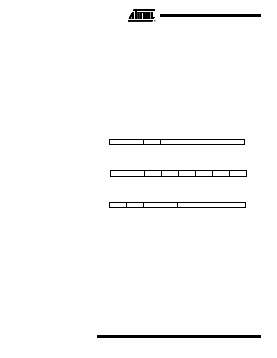
Port C Data Register – PORTC
Port C Data Direction Register
– DDRC
Port C Input Pins Address –
PINC
The Port C Input Pins address (PINC) is not a register; this address enables access to
the physical value on each Port C pin. When reading PORTC, the Port C Data Latch is
read and when reading PINC, the logical values present on the pins are read.
Port C as General Digital I/O
All eight pins in Port C have equal functionality when used as digital I/O pins.
PCn, general I/O pin: The DDCn bit in the DDRC Register selects the direction of this
pin. If DDCn is set (one), PCn is configured as an output pin. If DDCn is cleared (zero),
PCn is configured as an input pin. If PORTCn is set (one) when the pin is configured as
an input pin, the MOS pull-up resistor is activated. To switch the pull-up resistor off,
PORTCn has to be cleared (zero) or the pin has to be configured as an output pin. The
Port C pins are tri-stated when a reset condition becomes active, even if the clock is not
running.
Bit
7
6
5
4
3
2
1
0
$15 ($35)
PORTC7
PORTC6
PORTC5
PORTC4
PORTC3
PORTC2
PORTC1
PORTC0
PORTC
Read/Write
R/W
R/W
R/W
R/W
R/W
R/W
R/W
R/W
Initial Value
0
0
0
0
0
0
0
0
Bit
7
6
5
4
3
2
1
0
$14 ($34)
DDC7
DDC6
DDC5
DDC4
DDC3
DDC2
DDC1
DDC0
DDRC
Read/Write
R/W
R/W
R/W
R/W
R/W
R/W
R/W
R/W
Initial Value
0
0
0
0
0
0
0
0
Bit
7
6
5
4
3
2
1
0
$13 ($33)
PINC7
PINC6
PINC5
PINC4
PINC3
PINC2
PINC1
PINC0
PINC
Read/Write
R
R
R
R
R
R
R
R
Initial Value
N/A
N/A
N/A
N/A
N/A
N/A
N/A
N/A