Serial downloading, Atmega161(l) – Rainbow Electronics ATmega161L User Manual
Page 125
125
ATmega161(L)
1228C–AVR–08/02
Notes:
1. t
WLRH
is valid for the Write EEPROM, Write Fuse bits and Write Lock bits commands.
2. t
WLRH_CE
is valid for the Chip Erase command.
3. t
WLRH_FLASH
is valid for the Write Flash command.
Serial Downloading
Both the Flash and EEPROM memory arrays can be programmed using the serial SPI
bus while RESET is pulled to GND. The serial interface consists of pins SCK, MOSI
(input) and MISO (output). After RESET is set low, the Programming Enable instruction
needs to be executed first, before program/erase operations can be executed.
When programming the EEPROM, an auto-erase cycle is built into the self-timed pro-
gramming operation (in the Serial mode ONLY) and there is no need to first execute the
Chip Erase instruction. The chip erase operation turns the contents of every memory
location in both the program and EEPROM arrays into $FF.
The program and EEPROM memory arrays have separate address spaces:
$0000 to $1FFF for Program memory and $0000 to $01FF for EEPROM memory.
Either an external system clock is supplied at pin XTAL1 or a crystal needs to be con-
nected across pins XTAL1 and XTAL2. The minimum low and high periods for the serial
clock (SCK) input are defined as follows:
Low: > 2 XTAL1 clock cycles
High: > 2 XTAL1 clock cycles
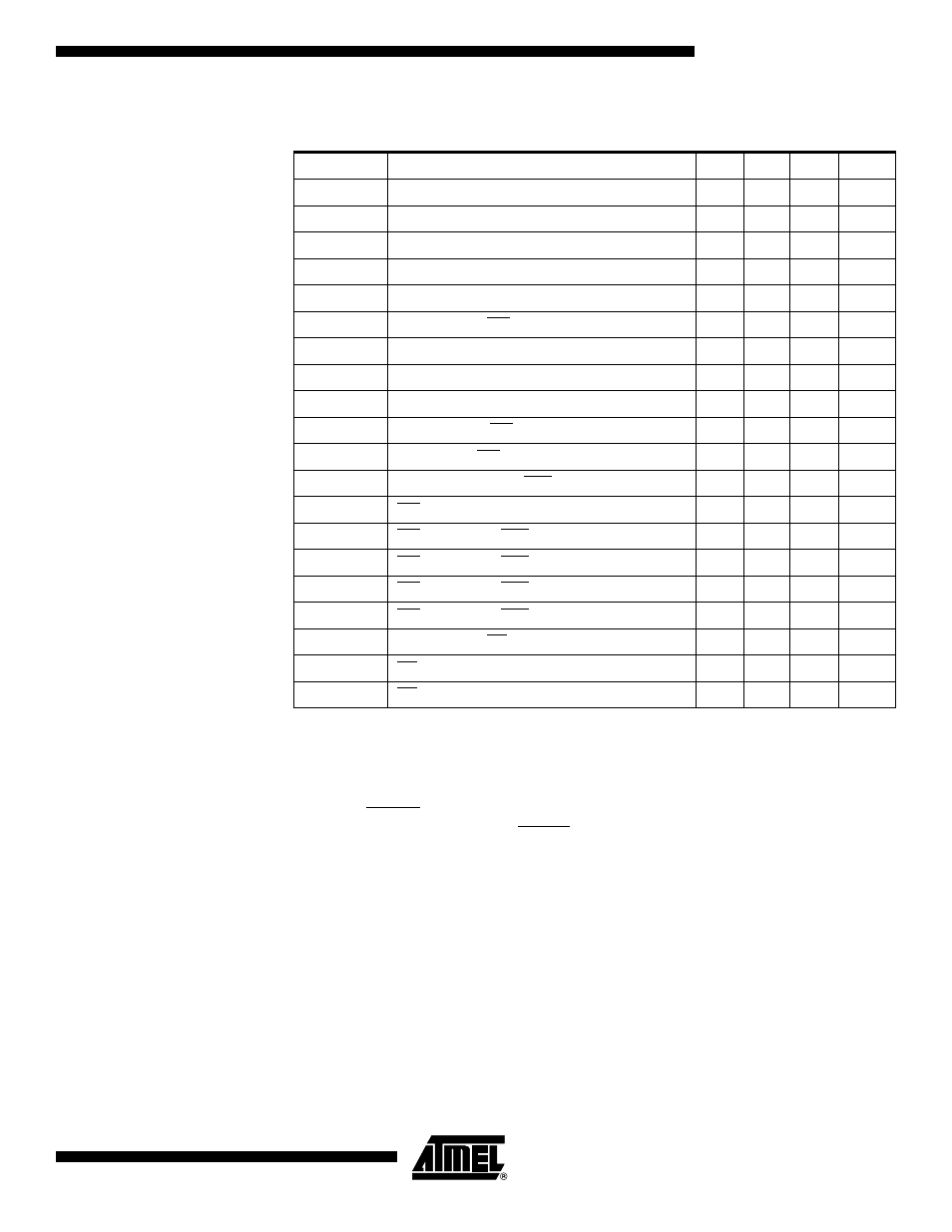
Table 45. Parallel Programming Characteristics, T
A
= 25
°C ± 10%, V
CC
= 5V ±
10%
(1)(2)(3)
Symbol
Parameter
Min
Typ
Max
Units
V
PP
Programming Enable Voltage
11.5
12.5
V
I
PP
Programming Enable Current
250
µA
t
DVXH
Data and Control Valid before XTAL1 High
67
ns
t
XHXL
XTAL1 Pulse Width High
67
ns
t
XLDX
Data and Control Hold after XTAL1 Low
67
ns
t
XLWL
XTAL1 Low to WR Low
67
ns
t
BVXH
BS1 Valid before XTAL1 High
67
ns
t
PHPL
PAGEL Pulse Width High
67
ns
t
PLBX
BS1 Hold after PAGEL Low
67
ns
t
PLWL
PAGEL Low to WR Low
67
ns
t
BVWL
BS1 Valid to WR Low
67
ns
t
RHBX
BS1 Hold after RDY/BSY High
67
ns
t
WLWH
WR Pulse Width Low
67
ns
t
WLRL
WR Low to RDY/BSY Low
0
2.5
µs
t
WLRH
WR Low to RDY/BSY High
(1)
1
1.7
ms
t
WLRH_CE
WR Low to RDY/BSY High for Chip Erase
(2)
16
28
ms
t
WLRH_FLASH
WR Low to RDY/BSY High for Write Flash
(3)
8
14
ms
t
XLOL
XTAL1 Low to OE Low
67
ns
t
OLDV
OE Low to DATA Valid
20
ns
t
OHDZ
OE High to DATA Tri-stated
20
ns