Port e, Port e data register – porte, Port e data direction register – ddre – Rainbow Electronics ATmega161L User Manual
Page 106: Port e input pins address – pine, Port e as general digital i/o, Atmega161(l)
106
ATmega161(L)
1228C–AVR–08/02
Port E
Port E is a 3-bit bi-directional I/O port with internal pull-up resistors.
Three I/O address locations are allocated for the Port E, one each for the Data Register
– PORTE, $07($27), Data Direction Register – DDRE, $06($26) and the Port E Input
Pins – PINE, $05($25). The Port E Input Pins address is read-only, while the Data Reg-
ister and the Data Direction Register are read/write.
The Port E output buffers can sink 20 mA. As inputs, Port E pins that are externally
pulled low will source current if the pull-up resistors are activated.
Port E pins have alternate functions as shown in Table 35.
Note:
1. When the PE1 pin is used for the alternate function, the DDRE and PORTE Registers
have to be set according to the alternate function description.
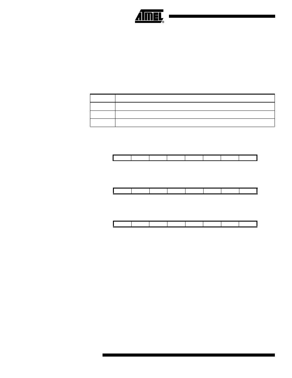
Port E Data Register – PORTE
Port E Data Direction Register
– DDRE
Port E Input Pins Address –
PINE
The Port E Input Pins address (PINE) is not a register; this address enables access to
the physical value on each Port E pin. When reading PORTE, the Port E Data Latch is
read and when reading PINE, the logical values present on the pins are read.
Port E as General Digital I/O
PEn, general I/O pin: The DDEn bit in the DDRE Register selects the direction of this
pin. If DDEn is set (one), PEn is configured as an output pin. If DDEn is cleared (zero),
PEn is configured as an input pin. If PORTEn is set (one) when configured as an input
pin, the MOS pull-up resistor is activated. To switch the pull-up resistor off, the PORTEn
has to be cleared (zero) or the pin has to be configured as an output pin. The Port E pins
are tri-stated when a reset condition becomes active, even if the clock is not running.
Table 35. Port E Pin Alternate Functions
(1)
Port Pin
Alternate Function
PE0
ICP (Input Capture Pin Timer/Counter1)/INT2 (External Interrupt 2 Input)
PE1
OC1B (Timer/Counter1 Output CompareB Match Output)
PE2
ALE (Address Latch Enable, External Memory)
Bit
7
6
5
4
3
2
1
0
$07 ($27)
–
–
–
–
–
PORTE2
PORTE1
PORTE0
PORTE
Read/Write
R
R
R
R
R
R/W
R/W
R/W
Initial Value
0
0
0
0
0
0
0
0
Bit
7
6
5
4
3
2
1
0
$06 ($26)
–
–
–
–
–
DDE2
DDE1
DDE0
DDRE
Read/Write
R
R
R
R
R
R/W
R/W
R/W
Initial Value
0
0
0
0
0
0
0
0
Bit
7
6
5
4
3
2
1
0
$05 ($25)
–
–
–
–
–
PINE2
PINE1
PINE0
PINE
Read/Write
R
R
R
R
R
R
R
R
Initial Value
0
0
0
0
0
N/A
N/A
N/A