Multi-processor communication mode, Uart control, Uart0 i/o data register – udr0 – Rainbow Electronics ATmega161L User Manual
Page 73: Uart1 i/o data register – udr1, Uart0 control and status registers – ucsr0a, Atmega161(l)
73
ATmega161(L)
1228C–AVR–08/02
Multi-processor
Communication Mode
The Multi-processor Communication mode enables several Slave MCUs to receive data
from a master MCU. This is done by first decoding an address byte to find out which
MCU has been addressed. If a particular Slave MCU has been addressed, it will receive
the following data bytes as normal, while the other Slave MCUs will ignore the data
bytes until another address byte is received.
For an MCU to act as a master MCU, it should enter 9-bit transmission mode (CHR9n in
UCSRnB set). The ninth bit must be one to indicate that an address byte is being trans-
mitted, and zero to indicate that a data byte is being transmitted.
For the Slave MCUs, the mechanism appears slightly different for 8-bit and 9-bit recep-
tion mode. In 8-bit reception mode (CHR9n in UCSRnB cleared), the stop bit is one for
an address byte and zero for a data byte. In 9-bit reception mode (CHR9n in UCSRnB
set), the ninth bit is one for an address byte and zero for a data byte, whereas the stop
bit is always high.
The following procedure should be used to exchange data in Multi-processor Communi-
cation mode:
1.
All Slave MCUs are in Multi-processor Communication mode (MPCMn in UCS-
RnA is set).
2.
The master MCU sends an address byte and all Slaves receive and read this
byte. In the Slave MCUs, the RXCn Flag in UCSRnA will be set as normal.
3.
Each Slave MCU reads the UDRn Register and determines if it has been
selected. If so, it clears the MPCMn bit in UCSRnA; otherwise, it waits for the
next address byte.
4.
For each received data byte, the receiving MCU will set the Receive Complete
Flag (RXCn in UCSRnA). In 8-bit mode, the receiving MCU will also generate a
framing error (FEn in UCSRnA set), since the stop bit is zero. The other Slave
MCUs, which still have the MPCMn bit set, will ignore the data byte. In this case,
the UDRn Register and the RXCn, FEn, or Flags will not be affected.
5.
After the last byte has been transferred, the process repeats from step 2.
UART Control
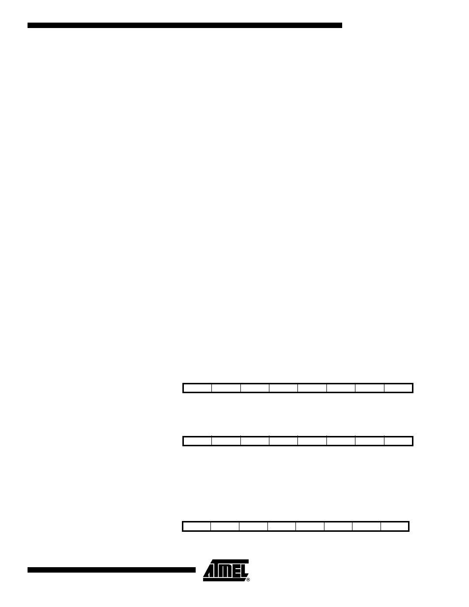
UART0 I/O Data Register –
UDR0
UART1 I/O Data Register –
UDR1
The UDRn Register is actually two physically separate registers sharing the same I/O
address. When writing to the register, the UART Transmit Data Register is written.
When reading from UDRn, the UART Receive Data Register is read.
UART0 Control and Status
Registers – UCSR0A
Bit
7
6
5
4
3
2
1
0
$0C ($2C)
MSB
LSB
UDR0
Read/Write
R/W
R/W
R/W
R/W
R/W
R/W
R/W
R/W
Initial Value
0
0
0
0
0
0
0
0
Bit
7
6
5
4
3
2
1
0
$03 ($23)
MSB
LSB
UDR1
Read/Write
R/W
R/W
R/W
R/W
R/W
R/W
R/W
R/W
Initial Value
0
0
0
0
0
0
0
0
Bit
7
6
5
4
3
2
1
0
$0B ($2B)
RXC0
TXC0
UDRE0
FE0
OR0
–
U2X0
MPCM0
UCSR0A
Read/Write
R
R/W
R
R
R
R
R/W
R/W
Initial Value
0
0
1
0
0
0
0
0