Atmega161(l) – Rainbow Electronics ATmega161L User Manual
Page 46

46
ATmega161(L)
1228C–AVR–08/02
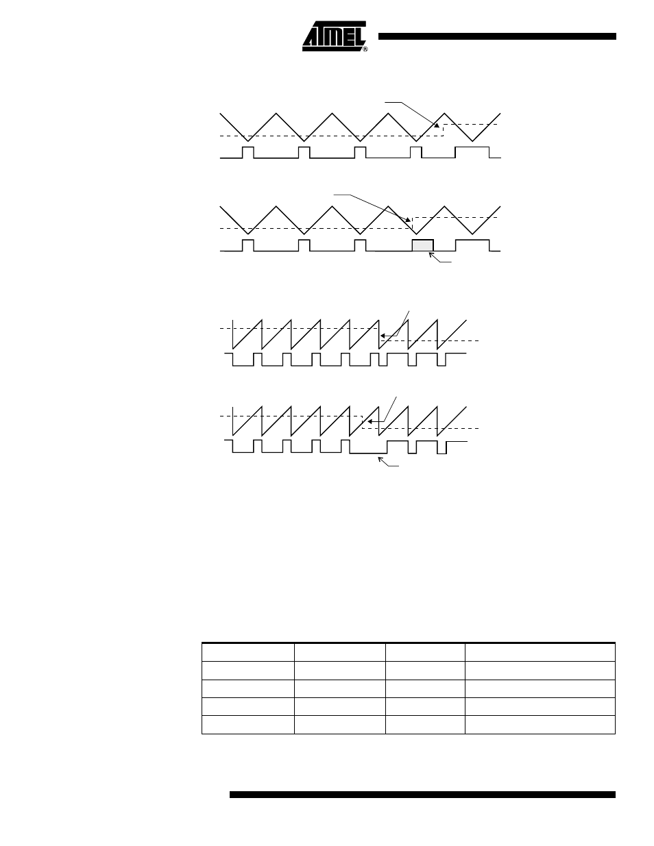
Figure 33. Effects of Unsynchronized OCR Latching in Up/Down Mode
Figure 34. Effects of Unsynchronized OCR Latching in Overflow Mode.
Note:
n = 0 or 2 (Figure 33 and Figure 34)
During the time between the write and the latch operation, a read from the Output Com-
pare Registers will read the contents of the temporary location. This means that the
most recently written value always will read out of OCR0 and OCR2.
When the Output Compare Register contains $00 or $FF, and the up/down PWM mode
is selected, the output PB0(OC0/PWM0)/PB1(OC2/PWM2) is updated to low or high on
the next compare match according to the settings of COMn1/COMn0. This is shown in
Table 13. In overflow PWM mode, the output PB0(OC0/PWM0)/PB1(OC2/PWM2) is
held low or high only when the Output Compare Register contains $FF.
Note:
1. n = 0 or 2
2. In overflow PWM mode, the table above is only valid for OCRn = $FF.
Table 13. PWM Outputs OCRn = $00 or $FF
(1)(2)
COMn1
COMn0
OCRn
Output PWMn
1
0
$00
L
1
0
$FF
H
1
1
$00
H
1
1
$FF
L
PWM Output OCn
PWM Output OCn
Unsynchronized OCn Latch
Synchronized OCn Latch
Compare Value changes
Counter Value
Compare Value
Glitch
Counter Value
Compare Value
Compare Value changes
PWM Output OCn
PWM Output OCn
Unsynchronized OCn Latch
Synchronized OCn Latch
Counter Value
Compare Value
Counter Value
Compare Value
Compare Value changes
Compare Value changes
Glitch
