Data reception, Atmega161(l) – Rainbow Electronics ATmega161L User Manual
Page 71
71
ATmega161(L)
1228C–AVR–08/02
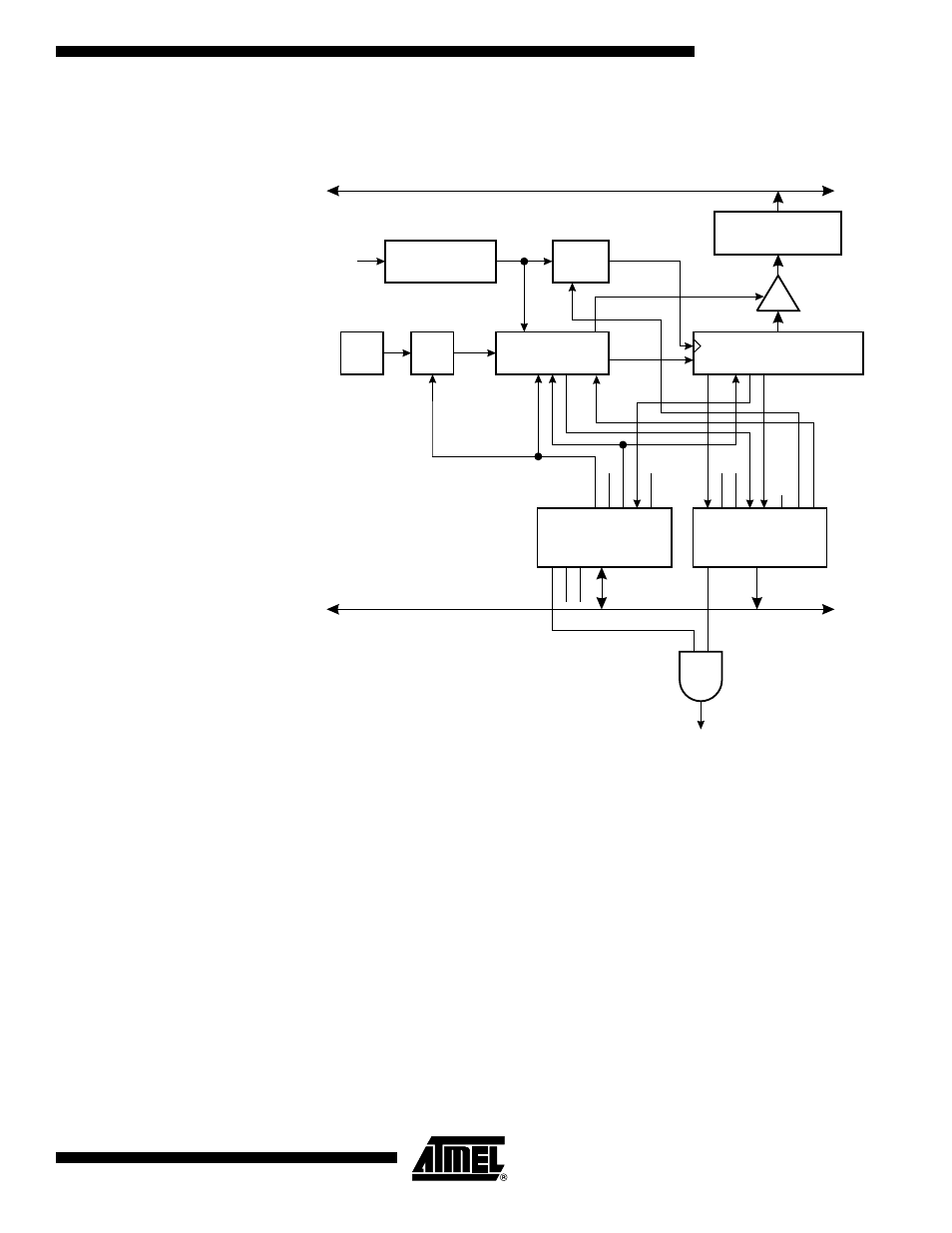
Data Reception
Figure 45 shows a block diagram of the UART Receiver.
Figure 45. UART Receiver
The Receiver front-end logic samples the signal on the RXDn pin at a frequency 16
times the baud rate. While the line is idle, one single sample of logical “0” will be inter-
preted as the falling edge of a start bit, and the start bit detection sequence is initiated.
Let sample 1 denote the first zero-sample. Following the 1-to-0 transition, the Receiver
samples the RXDn pin at samples 8, 9 and 10. If two or more of these three samples are
found to be logical “1”s, the start bit is rejected as a noise spike and the Receiver starts
looking for the next 1-to-0 transition.
If, however, a valid start bit is detected, sampling of the data bits following the start bit is
performed. These bits are also sampled at samples 8, 9 and 10. The logical value found
in at least two of the three samples is taken as the bit value. All bits are shifted into the
Transmitter Shift Register as they are sampled. Sampling of an incoming character is
shown in Figure 46. Note that the description above is not valid when the UART trans-
mission speed is doubled. See “Double-speed Transmission” on page 78 for a detailed
description.
PD0/
PB2
DATA BUS
BAUD
UART I/O DATA
REGISTER (UDRn)
10(11)-BIT RX
SHIFT REGISTER
STORE UDRn
/16
BAUD x 16
RXENn
TXENn
CHR9n
RXB8n
TXB8n
U2Xn
RXCn
TXCn
UDREn
FEn
MPCMPn
ORn
UART CONTROL AND
STATUS REGISTER
(UCSRnB)
UART CONTROL AND
STATUS REGISTER
(UCSRnA)
RXCIEn
TXCIEn
UDRIEn
TXCn
DATA BUS
PIN CONTROL
LOGIC
BAUD RATE
GENERATOR
XTAL
n = 0,1
RXCn
IRQ
DATA RECOVERY
LOGIC
RXDn