Fill the temporary buffer, Addressing the flash during self-programming, Atmega161(l) – Rainbow Electronics ATmega161L User Manual
Page 113
113
ATmega161(L)
1228C–AVR–08/02
Fill the Temporary Buffer
To write an instruction word, set up the address in the Z-pointer and data in R1:R0, write
“0001” to SPMCR, and execute SPM within four clock cycles after writing SPMCR. The
content of Z6:Z1 is used to address the data in the temporary buffer. Z13:Z7 must point
to the page that is supposed to be written.
Perform a Page Write
To execute a page write, set up the address in the Z-pointer, write “0101” to SPMCR,
and execute SPM within four clock cycles after writing SPMCR. The data in R1 and R0
are ignored. The page address must be written to Z13:Z7. During this operation, Z6:Z0
must be zero to ensure that the page is written correctly. When a page write operation is
completed, the Z-pointer will point to the first word in the successive page.
Addressing the FLASH during
Self-programming
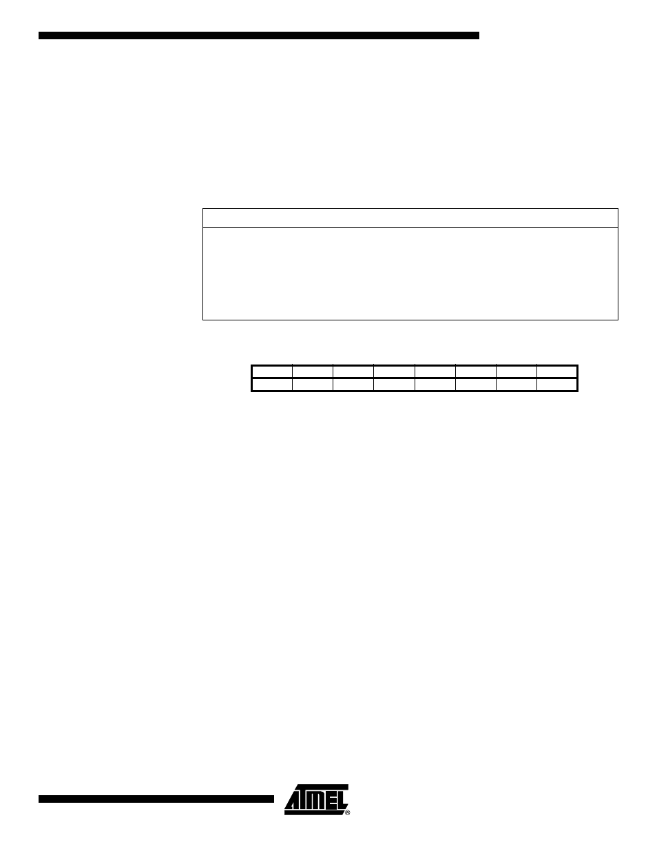
The Z-pointer is used to address the SPM commands.
Z15:Z14 always ignored
Z13:Z7
page select, for page erase, page write
Z6:Z1
word select, for filling temp buffer (must be zero during page write operation)
Z0
should be zero for all SPM commands, byte select for the LPM instruction
The only operation that does not use the Z-pointer is setting the Boot Loader Lock bits.
The content of the Z-pointer is ignored and will have no effect on the operation.
Note that the page erase and page write operation are addressed independently. There-
fore, it is of major importance that the Boot Loader software addresses the same page in
both the page erase and page write operations.
The LPM instruction also uses the Z-pointer to store the address. Since this instruction
addresses the Flash byte-by-byte, the LSB (bit Z0) of the Z-pointer is also used. See
page 16 for a detailed description.
Accidental writing into Flash program by the SPM instruction is prevented by setting up
an “SPM enable time window”. All accesses are executed by first setting I/O bits, and
then by executing SPM within four clock cycles. The I/O Register that controls the SPM
accesses is defined below.
Code Example
Wait:
in
r16,SPMCR
; read SPMCR Register
sbrc
r16,SPMEN
; Wait for SPMEN to be cleared (indicates that previous
write operation is completed)
rjmp
Wait
; if not cleared, keep waiting
ldi
r16,(1< set up for next erase out SPMCR,r16 ; output to register spm ; start the erase operation Bit 15 14 13 12 11 10 9 8 $1F ($1F) Z15 Z14 Z13 Z12 Z11 Z10 Z9 Z8 ZH $1E ($1E) Z7 Z6 Z5 Z4 Z3 Z2 Z1 Z0 ZL 7 6 5 4 3 2 1 0