I/o ports, Port a, Port a data register – porta – Rainbow Electronics ATmega161L User Manual
Page 89: Port a data direction register – ddra, Port a input pins address – pina, Port a as general digital i/o, Atmega161(l)
89
ATmega161(L)
1228C–AVR–08/02
I/O Ports
All AVR ports have true read-modify-write functionality when used as general digital I/O
ports. This means that the direction of one port pin can be changed without unintention-
ally changing the direction of any other pin with the SBI and CBI instructions. The same
applies for changing drive value (if configured as output) or enabling/disabling of pull-up
resistors (if configured as input).
Port A
Port A is an 8-bit bi-directional I/O port.
Three I/O memory address locations are allocated for the Port A, one each for the Data
Register – PORTA, $1B($3B), Data Direction Register – DDRA, $1A($3A) and the Port
A Input Pins – PINA, $19($39). The Port A Input Pins address is read-only, while the
Data Register and the Data Direction Register are read/write.
All port pins have individually selectable pull-up resistors. The Port A output buffers can
sink 20 mA and thus drive LED displays directly. When pins PA0 to PA7 are used as
inputs and are externally pulled low, they will source current if the internal pull-up resis-
tors are activated.
The Port A pins have alternate functions related to the optional external memory inter-
face. Port A can be configured to be the multiplexed low-order address/data bus during
accesses to the external Data memory. In this mode, Port A has internal pull-up
resistors.
When Port A is set to the alternate function by the SRE (External SRAM Enable) bit in
the MCUCR (MCU Control Register), the alternate settings override the Data Direction
Register.
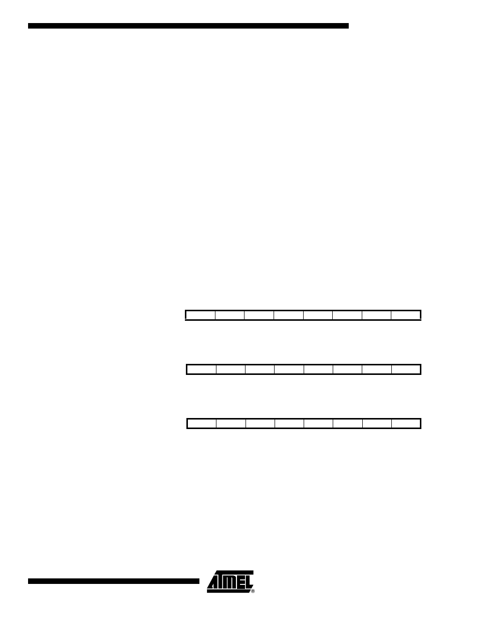
Port A Data Register – PORTA
Port A Data Direction Register
– DDRA
Port A Input Pins Address –
PINA
The Port A Input Pins address (PINA) is not a register; this address enables access to
the physical value on each Port A pin. When reading PORTA, the Port A Data Latch is
read and when reading PINA, the logical values present on the pins are read.
Port A as General Digital I/O
All eight pins in Port A have equal functionality when used as digital I/O pins.
PAn, general I/O pin: The DDAn bit in the DDRA Register selects the direction of this
pin. If DDAn is set (one), PAn is configured as an output pin. If DDAn is cleared (zero),
PAn is configured as an input pin. If PORTAn is set (one) when the pin is configured as
an input pin, the MOS pull-up resistor is activated. To switch the pull-up resistor off, the
PORTAn has to be cleared (zero) or the pin has to be configured as an output pin. The
Bit
7
6
5
4
3
2
1
0
$1B ($3B)
PORTA7
PORTA6
PORTA5
PORTA4
PORTA3
PORTA2
PORTA1
PORTA0
PORTA
Read/Write
R/W
R/W
R/W
R/W
R/W
R/W
R/W
R/W
Initial Value
0
0
0
0
0
0
0
0
Bit
7
6
5
4
3
2
1
0
$1A ($3A)
DDA7
DDA6
DDA5
DDA4
DDA3
DDA2
DDA1
DDA0
DDRA
Read/Write
R/W
R/W
R/W
R/W
R/W
R/W
R/W
R/W
Initial Value
0
0
0
0
0
0
0
0
Bit
7
6
5
4
3
2
1
0
$19 ($39)
PINA7
PINA6
PINA5
PINA4
PINA3
PINA2
PINA1
PINA0
PINA
Read/Write
R
R
R
R
R
R
R
R
Initial Value
N/A
N/A
N/A
N/A
N/A
N/A
N/A
N/A